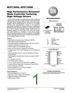
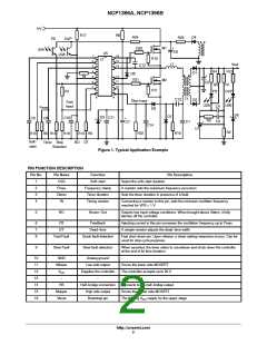
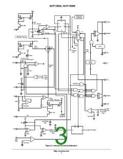
NCP1396A, NCP1396B
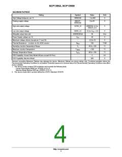
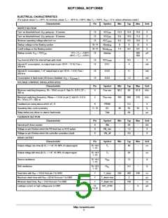
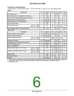
MAXIMUM RATINGS
Rating
Symbol
Value
--1 to 600
0 to 20
Unit
V
High Voltage bridge pin, pin 14
Floating supply voltage
VBRIDGE
VBOOT--
VBRIDGE
V
High side output voltage
VDRV_HI
VBRIDGE--0.3 to
VBOOT+0.3
V
Low side output voltage
VDRV_LO
--0.3 to V + 0.3
CC
V
V/ns
V
Allowable output slew rate
Power Supply voltage, pin 12
dVBRIDGE/dt
50
20
V
CC
Maximum voltage, all pins (except pin 11 and 10)
Thermal Resistance -- Junction--to--Air, SOIC version
Operating Junction Temperature Range
Maximum Junction Temperature
--
--0.3 to 10
130
V
R
C/W
C
θ
JA
T
J
--40 to +125
+150
T
C
JMAX
Storage Temperature Range
T
--60 to +150
2
C
STG
ESD Capability, Human Body Model (All pins except HV Pins)
ESD Capability, Machine Model
--
kV
V
--
200
Stresses exceeding Maximum Ratings may damage the device. Maximum Ratings are stress ratings only. Functional operation above the
Recommended Operating Conditions is not implied. Extended exposure to stresses above the Recommended Operating Conditions may affect
device reliability.
1. This device series contains ESD protection and exceeds the following tests:
Human Body Model 2000V per JESD22--A114--B
Machine Model Method 200V per JESD22--A115--A.
2. This device meets latch--up tests defined by JEDEC Standard JESD78.
http://onsemi.com
4

 ONSEMI [ ONSEMI ]