NCP1396A, NCP1396B
500
450
400
350
300
250
200
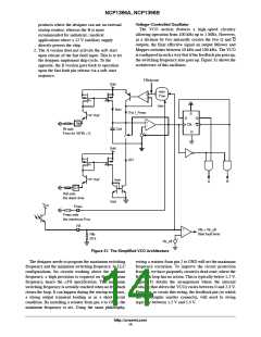
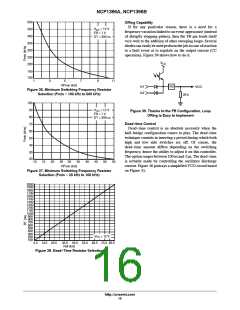
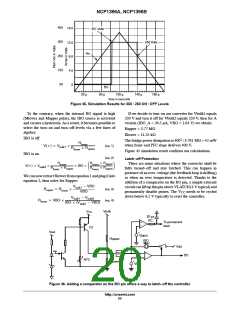
ORing Capability
If for any particular reason, there is a need for a
V
= 12 V
CC
frequency variation linked to an event appearance (instead
of abruptly stopping pulses), then the FB pin lends itself
very well to the addition of other sweeping loops. Several
diodescan easilybe usedperform the job incase ofreaction
to a fault event or to regulate on the output current (CC
operation). Figure 39 shows how to do it.
FB = 1 V
DT = 300 ns
V
CC
150
100
1
3
5
7
9
11
RFmin (kΩ)
In1
In2
FB
VCO
Figure 36. Minimum Switching Frequency Resistor
Selection (Fmin = 100 kHz to 500 kHz)
20 k
100
V
= 12 V
90
80
70
60
50
40
CC
Figure 39. Thanks to the FB Configuration, Loop
ORing is Easy to Implement
FB = 1 V
DT = 300 ns
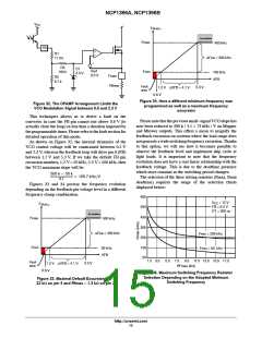
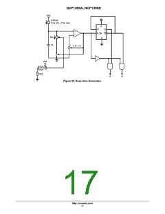
Dead--time Control
Dead-time control is an absolute necessity when the
half-bridge configuration comes to play. The dead-time
technique consists in inserting a period during which both
high and low side switches are off. Of course, the
dead-time amount differs depending on the switching
frequency, hence the ability to adjust it on this controller.
The option ranges between 100 ns and 2 ms. The dead-time
is actually made by controlling the oscillator discharge
current. Figure 40 portrays a simplified VCO circuit based
on Figure 31.
30
20
10
15
20
25 30
RFmin (kΩ)
35
40
45
50
55
Figure 37. Minimum Switching Frequency Resistor
Selection (Fmin = 20 kHz to 100 kHz)
2000
1900
1800
1700
1600
1500
1400
1300
1200
1100
1000
900
800
700
600
500
400
300
Vcc = 12 V
200
100
3.5 13.5 23.5
33.5 43.5 53.5 63.5 73.5 83.5
Rdt (kΩ)
Figure 38. Dead--Time Resistor Selection
http://onsemi.com
16

 ONSEMI [ ONSEMI ]