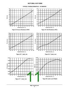
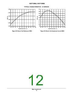
NCP1396A, NCP1396B
V
CC
FMu&Lu
No variations
Fmax
450 kHz
FB
+
--
R1
11.3 k
ΔFsw = 300 kHz
+
R3
100 k
R2
8.7 k
D1
2.3 V
Vref
0.5 V
Fmin
150 kHz
VFB
Fmax
Rfmax
Fault
area
5.3 V
1.2 V
ΔVFB = 4.1 V
0.6 V
Figure 34. Here a different minimum frequency was
programmed as well as a maximum frequency
excursion
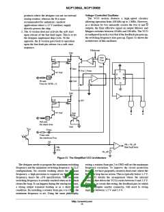
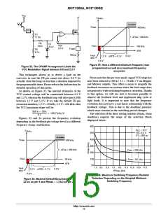
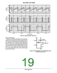
Figure 32. The OPAMP Arrangement Limits the
VCO Modulation Signal between 0.5 and 2.3 V
This techniques allows us to detect a fault on the
converter in case the FB pin cannot rise above 0.6 V (to
actually close the loop) in less than a duration imposed by
the programmable timer. Please referto the fault sectionfor
detailed operation of this mode.
As shown on Figure 32, the internal dynamics of the
VCO control voltage will be constrained between 0.5 V
and 2.3 V, whereas the feedback loop will drive pin 6 (FB)
between 1.2 V and 5.3 V. If we take the default FB pin
excursion numbers, 1.2 V = 50 kHz, 5.3 V = 500 kHz, then
the VCO maximum slope will be:
Please note that the previous small-signal VCO slope has
now been reduced to 300 k / 4.1 = 73 kHz / V on Mupper
and Mlower outputs. This offers a mean to magnify the
feedback excursion on systems where the load range does
not generate a wide switchingfrequency excursion. Thanks
to this option, we will see how it becomes possible to
observe the feedback level and implement skip cycle at
light loads. It is important to note that the frequency
evolution does not have a real linear relationship with the
feedback voltage. This is due to the deadtime presence
which stays constant as the switching period changes.
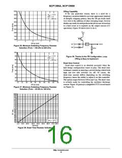
The selection of the three setting resistors (Fmax, Fmin
deadtime) requires the usage of the selection charts
displayed below:
500 k − 50 k
= 109.7 kHz∕V
4.1
Figures 33 and 34 portray the frequency evolution
depending on the feedback pin voltage level in a different
frequency clamp combination.
650
V
= 12 V
CC
FMu&Lu
550
450
350
250
FB = 6.5 V
DT = 300 ns
No variations
Fmax
500 kHz
ΔFsw = 450 kHz
Fmin = 200 kHz
Fmin
150
50
50 kHz
VFB
kHz
Fmin = 50
1.5 3.5
5.5 7.5
9.5 11.5 13.5 15.5 17.5
Fault
area
5.3 V
1.2 V
ΔVFB = 4.1 V
RFmax (kΩ)
0.6 V
Figure 35. Maximum Switching Frequency Resistor
Selection Depending on the Adopted Minimum
Switching Frequency
Figure 33. Maximal Default Excursion, Rt =
22 kΩ on pin 4 and Rfmax = 1.3 kΩ on pin 2
http://onsemi.com
15

 ONSEMI [ ONSEMI ]