NCP1252
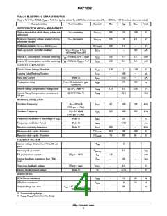
Table 4. ELECTRICAL CHARATERISTICS
(V = 15 V, R = 43 kW, C
= 1 nF. For typical values T = 25°C, for min/max values T = –25°C to +125°C, unless otherwise noted)
CC
T
DRV
J
J
Characteristics
Test Condition
Symbol
Min
Typ
Max
Unit
SUPPLY SECTION AND V MANAGEMENT
CC
Startup threshold at which driving pulses are
authorized
V
increasing
decreasing
V
V
9.4
8.4
10
9
10.6
9.6
V
V
CC
CC(on)
Minimum Operating voltage at which driving
pulses are stopped
V
CC
CC(off)
Hysteresis between V
and V
V
CC(HYS)
0.9
1.0
−
V
CC(on)
CC(min)
Start−up current, controller disabled
V
< V
& V
I
−
−
100
mA
CC
CC(on)
CC
CC1
increasing from zero
Internal IC consumption, controller switching
Internal IC consumption, controller switching
CURRENT COMPARATOR
F
=100 kHz, DRV = open
I
I
0.5
2.0
1.4
2.7
2.2
3.5
mA
mA
sw
sw
CC2
F
=100 kHz, C
= 1 nF
DRV
CC3
Current Sense Voltage Threshold
Leading Edge Blanking Duration
Input Bias Current
V
0.92
−
1
1.08
−
V
ILIM
t
160
0.02
70
ns
mA
ns
LEB
(Note 3)
I
−
−
bias
ILIM
Propagation delay
From CS detected to gate
turned off
t
−
150
Internal Ramp Compensation Voltage level
@ 25°C (Note 4)
@ 25°C (Note 4)
V
3.15
3.5
3.85
V
ramp
Internal Ramp Compensation resistance to
CS pin
R
−
26.5
−
kW
ramp
INTERNAL OSCILLATOR
Oscillator Frequency
R = 43 kW &
DRV pin = 47 kW
f
f
92
100
500
108
550
kHz
kHz
T
OSC
Oscillator Frequency
R = 8.5 kW &
T
425
OSC
DRV pin = 47 kW
Frequency Modulation in percentage of f
Frequency modulation Period
Maximum operating frequency
Maximum duty−cycle – A version
Maximum duty−cycle – B version
FEEDBACK SECTION
(Note 3)
f
−
−
5
3.33
−
−
−
%
ms
kHz
%
OSC
jitter
(Note 3)
T
swing
(Note 3)
f
500
45.6
76
−
MAX
DC
48
49.6
84
maxA
maxB
DC
80
%
Internal voltage division from FB to CS set-
point
FB
−
3
−
−
div
Internal pull−up resistor
R
−
1.5
−
3.5
−
−
−
−
kW
mA
kW
pull−up
FB pin maximum current
FB pin = GND
I
FB
Internal feedback impedance from FB to
GND
Z
FB
40
Open loop feedback voltage
Internal Diode forward voltage
DRIVE OUTPUT
FB pin = open
(Note 3)
V
−
−
6.0
−
−
V
V
FBOL
V
f
0.75
DRV Source resistance
DRV Sink resistance
R
−
−
−
10
6
30
19
−
W
W
SRC
R
SINK
Output voltage rise−time
V
CC
= 15 V, C
= 1nF,
t
r
26
ns
DRV
10 to 90%
3. Guaranteed by design
4. V
, R
Guaranteed by design
ramp
ramp
http://onsemi.com
4

 ONSEMI [ ONSEMI ]