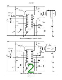
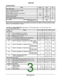
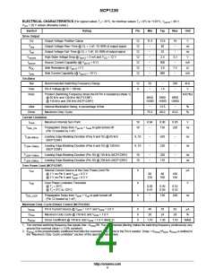
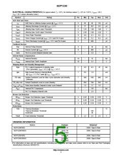
NCP1239
PIN FUNCTION DESCRIPTION
Pin No.
Pin Name
Function
Pin Description
1
GTS
Shuts the PFC down in
standby
The standby detection block changes Pin 1 state in accordance to the mode
(standby or normal mode). Pin1 is designed to drive an external pnp transistor that
connects or disconnects the NCP1239’s V to the PFC’s.
CC
2
REF5V
A 5V reference voltage
This pin helps to internally bias the controller but can also be used to power
surrounding logic gates for any purposes. The typical output current is 10 mA. This
voltage source is disabled during the circuit startup and latched−off phases. A
100 nF filtering capacitor must be placed between Pin 2 and ground.
3
4
5
6
Fault Detect
Rt
Enables to permanently
shutdown the part
If the Pin 3 voltage exceeds 2.4 V, the circuit is permanently shut down. This pin
can be used to monitor the voltage across a thermistor in order to protect the
application from excessive heating and/or to detect an overvoltage condition.
Timing resistor
Brown−Out
Pin 4 resistor allows a precise frequency programming. The circuit is optimized to
operate between 50 kHz and 150 kHz (NCP1239F) and between 100 kHz and
250 kHz (NCP1239V).
Brown−Out
SS/Timer
This pin receives a portion of the bulk capacitor to authorize operation above a
certain level of mains only. It also serves to elaborate an offset voltage on Pin 9
used for Over Power Compensation.
Performs soft−start and
fault timeout
During Power on and fault conditions, the capacitor connected to this pin ensures a
soft−start period. When a fault is detected, this pin is internally brought high by a
current source. If 4.3 V are reached, the fault is confirmed and the circuit enters an
auto−recovery burst mode, otherwise the pin goes back to a lower value and
oscillates to perform frequency jittering.
7
Skip Adjust
Adjust skip level
By adjusting the skip−cycle level, it is possible to fight against noisy transformers
and modify the standby detection thresholds. Keep Pin 7 open to operate with the
default levels (skip threshold setpoint: 140 mV, normal mode recovery setpoint:
250 mV).
8
9
FB
Feedback signal
An opto−coupler collector pulls this pin low to regulate
Over Power
Limit
Enables a precise peak
This pin delivers a current proportional to V , an image of the high voltage rail.
pin5
current clamp and then an Inserting a resistor between Pin 9 and the current sense resistor, an offset
(NCP1239F)
accurate Over Power
Detection
proportional to the input voltage is built. Such offset compensates the circuit and
power switch propagation delays for an accurate power limitation in the whole input
voltage range.
9
Max Duty−
Cycle
(NCP1239V)
Enables to precisely
clamp the maximum
duty−cycle.
This terminal sources a constant current. Connect a resistor between Pin 9 and
Ground to select the maximum duty−cycle.
10
CS
The current sense input
This pin receives the primary current information via a sense element. By inserting
a resistor in series with this pin, it becomes possible to introduce ramp
compensation.
11
12
Ground
Drv
The IC ground
−
Drives the MOSFET
By offering up to +500 mA/−800 mA peak, this pin lets you drive large Qg
MOSFET’s. It is clamped to 16 V maximum not to exceed the maximum
gate−source voltage of most power MOSFET’s.
13
14
15
16
V
Supplies the controller
This pin accepts up to 36 V from an auxiliary winding.
Creepage distance.
CC
NC
NC
HV
−
−
Creepage distance.
The high−voltage startup This pin connects to the bulk capacitor to generate the startup current.
http://onsemi.com
6

 ONSEMI [ ONSEMI ]