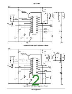
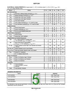
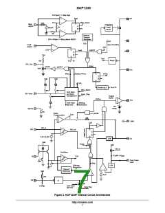
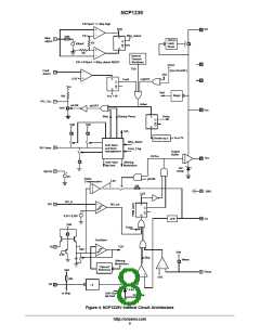
NCP1239
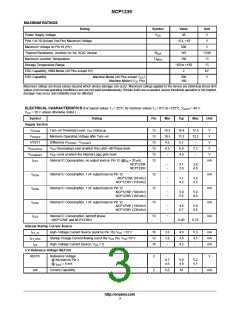
MAXIMUM RATINGS
Rating
Symbol
Value
36
Unit
V
Power Supply Voltage
V
CC
Pins 1 to 10 (except Vref Pin) Maximum Voltage
Maximum Voltage on Pin 16 (HV)
−0.3, +10
500
V
V
Thermal Resistance, Junction−to−Air, SOIC Version
Maximum Junction Temperature
R
145
°C/W
°C
°C
kV
V
ꢀ
JA
TJ
150
MAX
Storage Temperature Range
−60 to +150
2
ESD Capability, HBM Model (All Pins except HV)
ESD Capability
Machine Model (All Pins except V
)
200
160
CC
Machine Model (V Pin)
CC
Maximum ratings are those values beyond which device damage can occur. Maximum ratings applied to the device are individual stress limit
values (not normal operating conditions) and are not valid simultaneously. If these limits are exceeded, device functional operation is not implied,
damage may occur and reliability may be affected.
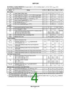
ELECTRICAL CHARACTERISTICS (For typical values T = 25°C, for min/max values T = 0°C to +125°C, V
= 48 V,
J
J
pin16
V
= 20 V unless otherwise noted.)
CC
Symbol
Supply Section
Rating
Pin
Min
Typ
Max
Unit
V
Turn−on Threshold Level, V Going up
13
13
13
13
13
13
15.5
10.5
4.5
6.5
−
16.4
11.2
5.1
17.5
12.2
−
V
V
CCON
CC
V
Minimum Operating Voltage after Turn−on
CCOFF
HYST1
Difference (V
− V
)
CCOFF
V
CCON
V
V
V
Decreasing Level at which the Latch−off Phase ends
Level at which the Internal Logic gets reset
6.9
7.2
−
V
CCLATCH
CCRESET
CC
CC
V
4.0
V
I
Internal IC Consumption, no output load on Pin 12 (@I = 20 ꢁ A)
mA
CC1
Rt
NCP1239F
NCP1239V
−
−
2.1
2.6
3.0
4.0
I
Internal IC Consumption, 1 nF output load on Pin 12
13
13
13
13
mA
mA
mA
mA
CC2a
CC2b
CC2c
NCP1239F (65 kHz)
NCP1239V (118 kHz)
−
−
3.1
4.2
3.8
6.5
I
I
Internal IC Consumption, 1 nF output load on Pin 12
NCP1239F (100 kHz)
NCP1239V (182 kHz)
−
−
3.9
5.5
5.0
8.5
Internal IC Consumption, 1 nF output load on Pin 12
NCP1239F (130 kHz)
NCP1239V (236 kHz)
−
−
4.6
6.7
5.9
9.6
I
Internal IC Consumption, latchoff phase
(NCP1239F and NCP1239V)
−
CC3
0.40
0.75
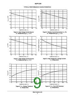
Internal Startup Current Source
High−Voltage Current Source (sunk by Pin 16), V = 10 V
I
16
13
16
2.0
1.8
−
4.0
3.6
4.2
5.3
4.5
−
mA
mA
mA
C1_hv
CC
I
Startup Charge Current flowing out of the V Pin, V =10 V
CC CC
C1_VCC
I
High−Voltage Current Source, V = 0
CC
C2
5 V Reference Voltage (REF5V)
REF5V
Iref
Reference Voltage
@ No load on Pin 2
2
2
V
4.7
4.6
5.0
4.9
5.2
5.1
@ I
= 5 mA
pin2
Current Capability
5.0
10
−
mA
http://onsemi.com
3

 ONSEMI [ ONSEMI ]