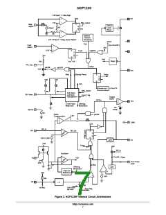
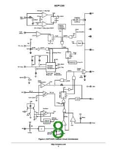
NCP1239
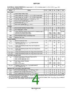
ELECTRICAL CHARACTERISTICS (For typical values T = 25°C, for min/max values T = 0°C to +125°C, V
= 48 V,
J
J
pin16
V
= 20 V unless otherwise noted.)
CC
Symbol
Rating
Pin
Min
Typ
Max
Unit
Drive Output
Vcl
Output Voltage Positive Clamp
12
12
12
12
12
12
12
11.5
−
13.6
40
16
−
V
ns
ns
V
T
rise
Output Voltage Rise−Time @ CL = 1 nF, 10−90% of output signal
Output Voltage Fall−Time @ CL = 1 nF, 10−90% of output signal
T
−
25
−
fall
V
High State Voltage Drop @ I
= 3 mA and V = 12 V
−
2.5
500
3.8
800
3.3
−
source
source
pin12
CC
I
Source Current Capability (@ V
= 0 V)
−
mA
ꢂ
pin12
R
OL
Sink Resistance @ V
=1 V
pin12
−
7.5
−
I
Sink Current Capability (@ V
= 10 V)
pin12
−
mA
sink
Oscillator
fsw
Recommended Switching Frequency Range
Pin 4 Voltage @ Rt = 100 k
12
4
25
−
−
250
−
kHz
V
Vosc
Kosc
ꢂ
1.6
Product (Switching Frequency times the Rt Pin 4 resistance) (Note 1)
@ 65 kHz and 130 kHz (NCP1239F)
kHz*kꢂ
6050
6500
6950
@ 118 kHz and 236 kHz (NCP1239V)
11000
11800
12600
ꢃ
f
s
w
Internal Modulation Swing, in percentage of fsw
Maximum Duty−Cycle
−
3.5
−
%
%
Dmax
75.5
80.0
83.0
Current Limitation
Maximum Internal Set−Point
I
10
10
0.84
−
0.90
130
0.95
220
V
Limit
T
Propagation Delay from V
(Pin 12 loaded by 1 nF)
> I to gate turned off
Limit
ns
DEL_CS
pin10
T
Leading Edge Blanking Duration (Pins 9 and 10) @ 65 kHz
(NCP1239F)
9, 10
9, 10
−
−
420
230
−
−
ns
ns
LEB−65kHz
T
Leading Edge Blanking Duration (Pins 9 and 10) @ 130 kHz
(NCP1239F)
LEB−130kHz
T
T
Leading Edge Blanking Duration (Pin 10) @ 118 kHz (NCP1239V)
Leading Edge Blanking Duration (Pin 10) @ 236 kHz (NCP1239V)
10
10
−
−
320
170
−
−
ns
ns
LEB−118kHz
LEB−236kHz
Over Power Limit (NCP1239F)
Internal Current Source of the Over Power Limit Pin
I
9
9
9
ꢁ A
V
ocp
@ 1 V on Pin 5 and V
@ 2 V on Pin 5 and V
= 0.5 V
= 0.5 V
60
120
80
160
100
185
pin9
pin9
V
opl
Over Power Limitation Threshold
@ T = 25°C
0.48
0.47
0.50
0.50
0.52
0.52
J
@ T = 0°C to 125°C
J
T
Propagation Delay from V
(Pin 12 loaded by 1 nF)
> V to gate turned off
−
130
220
ns
DEL_OCP
pin9
opl
Maximum Duty−Cycle (Dmax) Control (NCP1239V)
I
Pin 9 Current Source @ V
= 1.0 V and V = 2.0 V
pin9
9
9
9
46
20
55
24
63
29
ꢁ
A
Dmax
pin9
D
Maximum Duty Cycle @ 118 kHz and V
= 1.0 V
%
max
pin9
K
Dmax Coefficient @ 118 kHz and V
= 1.0 V (Note 2)
pin9
1.10
1.30
1.53
%/kꢂ
Dmax
1. The nominal switching frequency fsw equals: fsw = K /Rt. The implemented jittering makes the switching frequency continuously vary
OSC
around this nominal value ($3.5% variation).
Dmax
2. K
is the proportionality coefficient that links the maximum duty−cycle to the Pin 9 resistor: Dmax = K
*R
. K
is defined in
Dmax pin9 Dmax
the “Maximum Duty−Cycle Limitation” section of the operating description.
http://onsemi.com
4

 ONSEMI [ ONSEMI ]