MC74VHCT157A
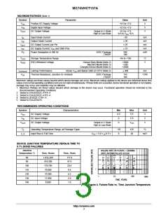
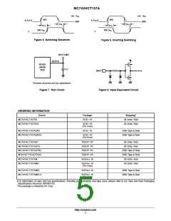
V
V
CC
CC
50%
50%
A, B or S
A, B or S
GND
GND
t
t
PHL
PHL
t
t
PLH
PLH
50% V
50% V
CC
CC
Y
Y
Figure 5. Switching Waveform
Figure 6. Inverting Switching
TEST POINT
OUTPUT
DEVICE
UNDER
C *
L
TEST
INPUT
*Includes all probe and jig capacitance
Figure 7. Test Circuit
Figure 8. Input Equivalent Circuit
ORDERING INFORMATION
Device
†
Package
Shipping
MC74VHCT157AD
MC74VHCT157ADG
SOIC−16
48 Units / Rail
48 Units / Rail
SOIC−16
(Pb−Free)
MC74VHCT157ADR2
MC74VHCT157ADR2G
SOIC−16
2500 Tape & Reel
2500 Tape & Reel
SOIC−16
(Pb−Free)
MC74VHCT157ADT
MC74VHCT157ADTG
MC74VHCT157ADTR2
M74VHCT157ADTR2G
MC74VHCT157AM
TSSOP−16*
TSSOP−16*
TSSOP−16*
TSSOP−16*
SOEIAJ−16
96 Units / Rail
96 Units / Rail
2500 Tape & Reel
2500 Tape & Reel
50 Units / Rail
MC74VHCT157AMG
SOEIAJ−16
(Pb−Free)
50 Units / Rail
MC74VHCT157AMEL
MC74VHCT157AMELG
SOEIAJ−16
2000 Tape & Reel
2000 Tape & Reel
SOEIAJ−16
(Pb−Free)
†For information on tape and reel specifications, including part orientation and tape sizes, please refer to our Tape and Reel Packaging
Specifications Brochure, BRD8011/D.
*This package is inherently Pb−Free.
http://onsemi.com
5

 ONSEMI [ ONSEMI ]