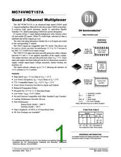
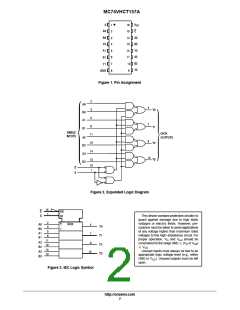
MC74VHCT157A
MAXIMUM RATINGS (Note 1)
Symbol
Parameter
Value
Unit
V
V
Positive DC Supply Voltage
Digital Input Voltage
−0.5 to +7.0
−0.5 to +7.0
−0.5 to +7.0
CC
V
V
IN
V
DC Output Voltage
Output in 3−State
V
OUT
High or Low State
−0.5 to V +0.5
CC
I
Input Diode Current
−20
$20
$25
$75
mA
mA
mA
mA
mW
IK
I
Output Diode Current
DC Output Current, per Pin
OK
I
OUT
I
DC Supply Current, V and GND Pins
CC
CC
P
Power Dissipation in Still Air
SOIC Package
TSSOP
200
180
D
T
V
Storage Temperature Range
ESD Withstand Voltage
−65 to +150
°C
STG
Human Body Model (Note 2)
Machine Model (Note 3)
>2000
>200
V
ESD
Charged Device Model (Note 4)
>2000
I
Latchup Performance
Above V and Below GND at 125°C (Note 5)
$300
mA
LATCHUP
CC
q
Thermal Resistance, Junction−to−Ambient
SOIC Package
TSSOP
143
164
°C/W
JA
Maximum ratings are those values beyond which device damage can occur. Maximum ratings applied to the device are individual stress limit
values (not normal operating conditions) and are not valid simultaneously. If these limits are exceeded, device functional operation is not implied,
damage may occur and reliability may be affected.
1. Maximum Ratings are those values beyond which damage to the device may occur. Functional operation should be restricted to the
Recommended Operating Conditions.
2. Tested to EIA/JESD22−A114−A
3. Tested to EIA/JESD22−A115−A
4. Tested to JESD22−C101−A
5. Tested to EIA/JESD78
RECOMMENDED OPERATING CONDITIONS
Symbol
Characteristics
Min
4.5
0
Max
5.5
Unit
V
V
DC Supply Voltage
DC Input Voltage
DC Output Voltage
CC
V
5.5
V
IN
V
Output in 3−State
High or Low State
0
V
V
OUT
CC
T
Operating Temperature Range, all Package Types
Input Rise or Fall Time
−55
0
125
20
°C
A
t , t
r
V = 5.0 V + 0.5 V
CC
ns/V
f
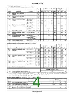
DEVICE JUNCTION TEMPERATURE VERSUS TIME TO
0.1% BOND FAILURES
Junction
Temperature °C
FAILURE RATE OF PLASTIC = CERAMIC
UNTIL INTERMETALLICS OCCUR
Time, Hours
Time, Years
80
1,032,200
419,300
178,700
79,600
37,000
17,800
8,900
117.8
47.9
20.4
9.4
90
100
110
120
130
140
1
4.2
1
10
100
1000
2.0
TIME, YEARS
1.0
Figure 4. Failure Rate vs. Time Junction Temperature
http://onsemi.com
3

 ONSEMI [ ONSEMI ]