MC74VHCT157A
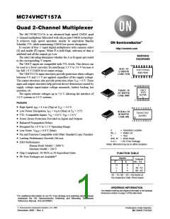
V
E
S
1
2
16
15
CC
A0
B0
Y0
A3
B3
Y3
A2
B2
Y2
3
4
14
13
A1
5
6
12
11
B1
7
8
10
Y1
GND
9
Figure 1. Pin Assignment
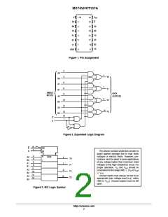
2
3
A0
B0
A1
B1
4
7
Y0
5
6
Y1
Y2
NIBBLE
INPUTS
DATA
OUTPUTS
11
10
14
13
A2
B2
A3
B3
9
12
Y3
15
1
E
S
Figure 2. Expanded Logic Diagram
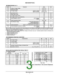
15
1
E
S
EN
G1
This device contains protection circuitry to
guard against damage due to high static
voltages or electric fields. However, pre-
cautions must be taken to avoid applications
of any voltage higher than maximum rated
voltages to this high−impedance circuit. For
2
3
5
6
MUX
A0
B0
A1
B1
1
1
4
7
Y0
Y1
Y2
Y3
proper operation, V and V
should be
in
out
11
10
14
13
A2
B2
9
constrained to the range GND v (V or V
)
in
out
v V
.
CC
Unused inputs must always be tied to an
appropriate logic voltage level (e.g., either
A3
B3
12
GND or V ). Unused outputs must be left
CC
open.
Figure 3. IEC Logic Symbol
http://onsemi.com
2

 ONSEMI [ ONSEMI ]