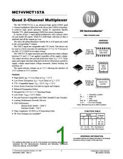
MC74VHCT157A
Quad 2−Channel Multiplexer
The MC74VHCT157A is an advanced high speed CMOS quad
2−channel multiplexer fabricated with silicon gate CMOS technology.
It achieves high speed operation similar to equivalent Bipolar
Schottky TTL while maintaining CMOS low power dissipation.
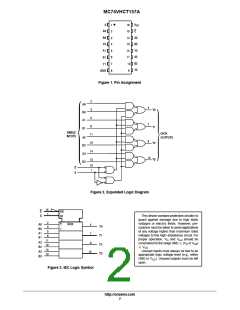
It consists of four 2−input digital multiplexers with common select
(S) and enable (E) inputs. When E is held High, selection of data is
inhibited and all the outputs go Low.
http://onsemi.com
MARKING
The select decoding determines whether the A or B inputs get routed
to the corresponding Y outputs.
DIAGRAMS
The VHCT inputs are compatible with TTL levels. This device can
be used as a level converter for interfacing 3.3 V to 5.0 V because it
has full 5.0 V CMOS level output swings.
The VHCT157A input structures provide protection when voltages
between 0 V and 5.5 V are applied, regardless of the supply voltage.
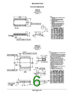
16
1
SOIC−16
D SUFFIX
CASE 751B
VHCT157AG
AWLYWW
1
The output structures also provide protection when V = 0 V. These
CC
input and output structures help prevent device destruction caused by
supply voltage−input/output voltage mismatch, battery backup, hot
insertion, etc.
The inputs tolerate voltages up to 7.0 V, allowing the interface of
5.0 V systems to 3.0 V systems.
16
VHCT
157A
ALYWG
G
TSSOP−16
DT SUFFIX
CASE 948F
1
1
Features
• High Speed: t = 4.1 ns (Typ) at V = 5.0 V
PD
CC
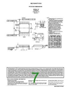
16
• Low Power Dissipation: I = 4 mA (Max) at T = 25°C
CC
A
SOEIAJ−16
M SUFFIX
CASE 966
74VHCT157
ALYWG
• TTL−Compatible Inputs: V = 0.8 V; V = 2.0 V
IL
IH
• Power Down Protection Provided on Inputs and Outputs
• Balanced Propagation Delays
1
1
• Designed for 2.0 V to 5.5 V Operating Range
A
WL, L
Y
= Assembly Location
= Wafer Lot
• Low Noise: V
= 0.8 V (Max)
OLP
• Pin and Function Compatible with Other Standard Logic Families
• Latchup Performance Exceeds 300 mA
= Year
WW, W = Work Week
G or G
= Pb−Free Package
• ESD Performance:
(Note: Microdot may be in either location)
Human Body Model > 2000 V;
Machine Model > 200 V
• Chip Complexity: 82 FETs or 20 Equivalent Gates
• Pb−Free Packages are Available*
FUNCTION TABLE
Inputs
Outputs
E
S
Y0 − Y3
H
L
L
X
L
H
L
A0−A3
B0−B3
A0 − A3, B0 − B3 = the levels of
the respective Data−Word Inputs.
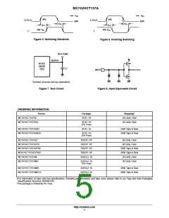
ORDERING INFORMATION
See detailed ordering and shipping information in the package
dimensions section on page 5 of this data sheet.
*For additional information on our Pb−Free strategy and soldering details, please
download the ON Semiconductor Soldering and Mounting Techniques
Reference Manual, SOLDERRM/D.
©
Semiconductor Components Industries, LLC, 2005
1
Publication Order Number:
December, 2005 − Rev. 2
MC74VHCT157A/D

 ONSEMI [ ONSEMI ]