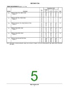
MC74HC175A
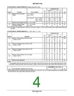
TIMING REQUIREMENTS (Input t = t = 6 ns)
r
f
Guaranteed Limit
– 55 to
V
CC
25_C
100
45
20
17
V
v 85_C v 125_C
Symbol
Parameter
Unit
t
Minimum Setup Time, Data to Clock
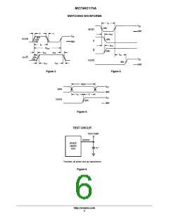
(Figure 3)
2.0
3.0
4.5
6.0
125
65
150
85
ns
su
25
30
21
26
t
Minimum Hold Time, Clock to Data
(Figure 3)
2.0
3.0
4.5
6.0
5
3
3
3
5
3
3
3
5
3
3
3
ns
ns
ns
ns
ns
h
t
Minimum Recovery Time, Reset Inactive to Clock
(Figure 2)
2.0
3.0
4.5
6.0
100
45
20
125
65
25
150
85
30
rec
17
21
26
t
t
Minimum Pulse Width, Clock
(Figure 1)
2.0
3.0
4.5
6.0
80
45
16
14
100
65
20
120
85
24
w
w
17
20
Minimum Pulse Width, Reset
(Figure 2)
2.0
3.0
4.5
6.0
80
45
16
14
100
65
20
120
85
24
17
20
t , t
r
Maximum Input Rise and Fall Times
(Figure 1)
2.0
3.0
4.5
6.0
1000
800
500
400
1000
800
500
400
1000
800
500
400
f
NOTE:Information on typical parametric values can be found in Chapter 2 of the ON Semiconductor High−Speed CMOS Data Book
(DL129/D).
http://onsemi.com
5

 ONSEMI [ ONSEMI ]