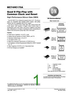
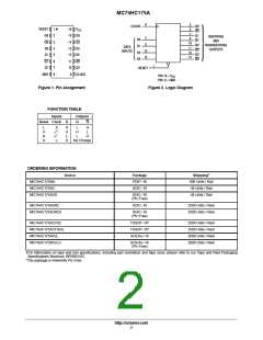
MC74HC175A
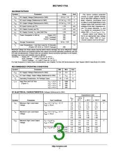
MAXIMUM RATINGS
Symbol
Parameter
Value
Unit
V
This device contains protection
circuitry to guard against damage
due to high static voltages or electric
fields. However, precautions must
be taken to avoid applications of any
voltage higher than maximum rated
voltages to this high−impedance cir-
V
DC Supply Voltage (Referenced to GND)
DC Input Voltage (Referenced to GND)
DC Output Voltage (Referenced to GND)
DC Input Current, per Pin
– 0.5 to + 7.0
CC
V
– 0.5 to V + 0.5
V
in
CC
V
– 0.5 to V + 0.5
V
out
CC
I
20
25
50
mA
mA
mA
mW
in
cuit. For proper operation, V and
in
I
I
DC Output Current, per Pin
out
V
out
should be constrained to the
range GND v (V or V ) v V
.
CC
DC Supply Current, V and GND Pins
in
out
CC
CC
Unused inputs must always be
tied to an appropriate logic voltage
P
Power Dissipation in Still Air,
Plastic DIP†
SOIC Package†
TSSOP Package†
750
500
450
D
level (e.g., either GND or V ).
CC
Unused outputs must be left open.
T
Storage Temperature
– 65 to + 150
_C
_C
stg
T
Lead Temperature, 1 mm from Case for 10 Seconds
(Plastic DIP, SOIC or TSSOP Package)
L
260
Maximum ratings are those values beyond which device damage can occur. Maximum ratings
applied to the device are individual stress limit values (not normal operating conditions) and are
not valid simultaneously. If these limits are exceeded, device functional operation is not implied,
damage may occur and reliability may be affected.
†Derating — Plastic DIP: – 10 mW/_C from 65_ to 125_C
SOIC Package: – 7 mW/_C from 65_ to 125_C
TSSOP Package: − 6.1 mW/_C from 65_ to 125_C
For high frequency or heavy load considerations, see Chapter 2 of the ON Semiconductor High−Speed CMOS Data Book (DL129/D).
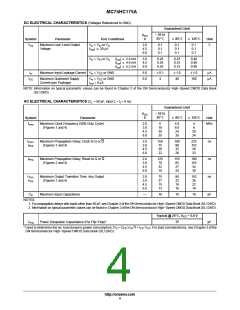
RECOMMENDED OPERATING CONDITIONS
Symbol
Parameter
Min
2.0
0
Max
Unit
V
V
DC Supply Voltage (Referenced to GND)
DC Input Voltage, Output Voltage (Referenced to GND)
Operating Temperature, All Package Types
6.0
CC
V , V
in out
V
V
CC
T
A
– 55
+ 125
_C
ns
t , t
r
Input Rise and Fall Time
(Figure 1)
V
V
V
V
= 2.0 V
= 3.0 V
= 4.5 V
= 6.0 V
0
0
0
1000
600
500
400
f
CC
CC
CC
CC
DC ELECTRICAL CHARACTERISTICS (Voltages Referenced to GND)
Guaranteed Limit
– 55 to
V
CC
25_C
1.5
2.1
3.15
4.2
V
v 85_C v 125_C
Symbol
Parameter
Test Conditions
= 0.1 V or V – 0.1 V
|I | v 20 mA
Unit
V
Minimum High−Level Input
Voltage
V
2.0
3.0
4.5
6.0
1.5
2.1
1.5
2.1
V
IH
out
CC
out
3.15
4.2
3.15
4 2
V
Maximum Low−Level Input
Voltage
V
= 0.1 V or V – 0.1 V
2.0
3.0
4.5
6.0
0.5
0.9
1.35
1.80
0.5
0.9
1.35
1.80
0.5
0.9
1.35
1.80
V
V
IL
out
CC
|I | v 20 mA
out
V
Minimum High−Level Output
Voltage
V
in
= V or V
IL
2.0
4.5
6.0
1.9
4.4
5.9
1.9
4.4
5.9
1.9
4.4
5.9
OH
IH
|I | v 20 mA
out
V
in
= V or V
|I | v 2.4 mA
3.0
4.5
6.0
2.48
3.98
5.48
2.34
3.84
5.34
2.20
3.70
5.20
IH
IL
out
|I | v 4.0 mA
out
|I | v 5.2 mA
out
http://onsemi.com
3

 ONSEMI [ ONSEMI ]