MC74HC175A
DC ELECTRICAL CHARACTERISTICS (Voltages Referenced to GND)
Guaranteed Limit
– 55 to
V
CC
25_C
0.1
0.1
0.1
v 85_C v 125_C
V
Symbol
Parameter
Test Conditions
= V or V
|I | v 20 mA
out
Unit
V
Maximum Low−Level Output
Voltage
V
in
2.0
4.5
6.0
0.1
0.1
0.1
0.1
0.1
0.1
V
OL
IH
IL
V
= V or V
|I | v 2.4 mA
3.0
4.5
6.0
0.26
0.26
0.26
0.33
0.33
0.33
0.40
0.40
0.40
in
IH
IL
out
|I | v 4.0 mA
out
|I | v 5.2 mA
out
I
Maximum Input Leakage Current
V
V
= V or GND
6.0
6.0
0.1
4
1.0
40
1.0
mA
mA
in
in
CC
I
Maximum Quiescent Supply
Current (per Package)
= V or GND
160
CC
in
CC
I
= 0 mA
out
NOTE:Information on typical parametric values can be found in Chapter 2 of the ON Semiconductor High−Speed CMOS Data Book
(DL129/D).
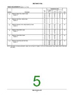
AC ELECTRICAL CHARACTERISTICS (C = 50 pF, Input t = t = 6 ns)
L
r
f
Guaranteed Limit
– 55 to
V
CC
25_C
V
v 85_C v 125_C
Symbol
Parameter
Unit
f
Maximum Clock Frequency (50% Duty Cycle)
(Figures 1 and 4)
2.0
3.0
4.5
6.0
6
4.8
8.0
24
4
6
MHz
max
10
30
35
20
24
28
t
t
,
Maximum Propagation Delay, Clock to Q or Q
(Figures 1 and 4)
2.0
3.0
4.5
6.0
150
75
26
190
90
32
225
110
38
ns
ns
ns
pF
PLH
PHL
22
28
33
t
Maximum Propagation Delay, Reset to Q or Q
(Figures 2 and 4)
2.0
3.0
4.5
6.0
125
70
22
155
85
27
190
110
34
PHL
19
24
30
t
t
,
Maximum Output Transition Time, Any Output
(Figures 1 and 4)
2.0
3.0
4.5
6.0
75
27
15
13
95
32
19
16
110
36
22
TLH
THL
19
C
in
Maximum Input Capacitance
—
10
10
10
NOTES:
1. For propagation delays with loads other than 50 pF, see Chapter 2 of the ON Semiconductor High−Speed CMOS Data Book (DL129/D).
2. Information on typical parametric values can be found in Chapter 2 of the ON Semiconductor High−Speed CMOS Data Book (DL129/D).
Typical @ 25°C, V = 5.0 V
CC
35
f + I V . For load considerations, see Chapter 2 of the
CC CC
C
Power Dissipation Capacitance (Per Flip−Flop)*
pF
PD
2
* Used to determine the no−load dynamic power consumption: P = C
V
D
PD CC
ON Semiconductor High−Speed CMOS Data Book (DL129/D).
http://onsemi.com
4

 ONSEMI [ ONSEMI ]