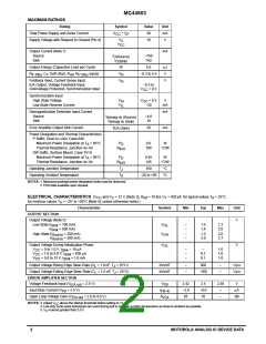
MC44603
ELECTRICAL CHARACTERISTICS (continued) (V
CC
and V = 12 V, [Note 3], R = 10 kΩ, C = 820 pF, for typical values T = 25°C,
C ref T A
for min/max values T = –25° to +85°C [Note 4], unless otherwise noted.)
A
Characteristic
Symbol
Min
Typ
Max
Unit
DEMAGNETIZATION DETECTION SECTION (Note 9)
Demagnetization Detect Input
Demagnetization Comparator Threshold (V
Decreasing)
V
50
–
–0.5
65
0.25
–
80
–
–
mV
µs
µA
Pin 9
Propagation Delay (Input to Output, Low to High)
demag–th
–
Input Bias Current (V
= 65 mV)
I
demag
Negative Clamp Level (I
demag–lb
= –2.0 mA)
C
–
–
–0.38
0.72
–
–
V
V
demag
L(neg)
L(pos)
Positive Clamp Level (I
= 2.0 mA)
SOFT–START SECTION (Note 11)
C
demag
Ratio Charge Current/I
I
/I
–
ref
ss(ch) ref
T
T
A
= 0° to +70°C
= –25° to +85°C
0.37
0.36
0.4
–
0.43
0.44
A
Discharge Current (V
Clamp Level
= 1.0 V)
I
1.5
2.2
5.0
2.4
–
mA
V
soft–start
discharge
V
2.6
ss(CL)
Duty Cycle (R
Duty Cycle (V
= 12 kΩ)
D
36
–
42
–
49
0
%
soft–start
soft–start (Pin 11)
soft–start 12k
D
soft–start
= 0.1 V)
OVERVOLTAGE SECTION
Protection Threshold Level on V
V
2.42
1.0
2.5
–
2.58
3.0
V
µs
V
OVP
OVP–th
Propagation Delay (V
Protection Level on V
> 2.58 V to V Low)
out
OVP
V
CC
CC prot
T
T
A
= 0° to +70°C
= –25° to +85°C
16.1
15.9
17
–
17.9
18.1
A
Input Resistance
–
kΩ
T
T
A
= 0° to +70°C
= –25° to +85°C
1.5
1.4
2.0
–
3.0
3.4
A
FOLDBACK SECTION (Note 10)
Current Sense Voltage Threshold (V
= 0.9 V)
V
0.86
–6.0
0.89
–2.0
0.9
–
V
foldback (Pin 5)
= 0 V)
CS–th
Foldback Input Bias Current (V
I
µA
foldback (Pin 5)
foldback–lb
STANDBY SECTION
Ratio I
/I
R P Stby ref
I
/I
–
–
R P Stby ref
T
A
= 0° to +70°C
0.37
0.36
0.4
–
0.43
0.44
T
A
= –25° to +85°C
Ratio Hysteresis (V Required to Return to Normal Operation from Standby
h
Operation)
V /V
h
R P Stby
T
T
A
= 0° to +70°C
= –25° to +85°C
1.42
1.4
1.5
–
1.58
1.6
A
Current Sense Voltage Threshold (V
= 1.0 V)
= 1.2 V)
V
0.28
0.31
0.34
V
V
R P Stby (Pin 12)
CS–Stby
CURRENT SENSE SECTION
Maximum Current Sense Input Threshold
(V = 2.3 V and V
V
CS–th
0.96
1.0
1.04
feedback (Pin 14) foldback (Pin 6)
Input Bias Current
I
–10
–
–2.0
120
–
µA
CS–ib
–
Propagation Delay (Current Sense Input to Output at V
MOS transistor = 3.0 V)
of
200
ns
TH
TOTAL DEVICE
Power Supply Current
I
mA
CC
Startup (V
Operating T = –25° to +85°C (Note 3)
= 13 V with V
Increasing)
–
13
0.3
17
0.45
20
CC
A
CC
Power Supply Zener Voltage (I
Thermal Shutdown
= 25 mA)
V
18.5
–
–
–
–
V
CC
Z
–
155
°C
NOTES: 13. Adjust V
above the startup threshold before setting to 12 V.
CC
14. Low duty cycle pulse techniques are used during test to maintain junction temperature as close to ambient as possible.
19. This function can be inhibited by connecting Pin 8 to Gnd. This allows a continuous current mode operation.
10. This function can be inhibited by connecting Pin 5 to V
11. The MC44603 can be shut down by connecting the Soft–Start pin (Pin 11) to Ground.
.
CC
4
MOTOROLA ANALOG IC DEVICE DATA

 ONSEMI [ ONSEMI ]