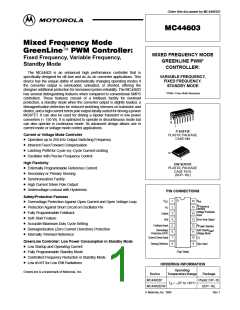
MC44603
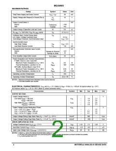
MAXIMUM RATINGS
Rating
Symbol
Value
30
Unit
mA
V
Total Power Supply and Zener Current
(I
CC
+ I )
Z
Supply Voltage with Respect to Ground (Pin 4)
V
18
C
V
CC
Output Current (Note 1)
mA
Source
Sink
I
–750
750
O(Source)
I
O(Sink)
Output Energy (Capacitive Load per Cycle)
W
5.0
µJ
V
R
, C , Soft–Start, R , R
F Stby ref P Stby
Inputs
V
V
–0.3 to 5.5
T
in
Foldback Input, Current Sense Input,
E/A Output, Voltage Feedback Input,
V
in
–0.3 to
Overvoltage Protection, Synchronization Input
V
V
+ 0.3
CC
Synchronization Input
High State Voltage
V
IH
+ 0.3
V
CC
Low State Reverse Current
V
IL
–20
mA
Demagnetization Detection Input Current
mA
Source
Sink
I
–4.0
10
demag–ib (Source)
I
demag–ib (Sink)
Error Amplifier Output Sink Current
I
20
mA
E/A (Sink)
Power Dissipation and Thermal Characteristics
P Suffix, Dual–In–Line, Case 648
Maximum Power Dissipation at T = 85°C
P
D
0.6
W
A
Thermal Resistance, Junction–to–Air
R
100
°C/W
θJA
DW Suffix, Surface Mount, Case 751G
Maximum Power Dissipation at T = 85°C
P
0.45
145
W
°C/W
A
D
Thermal Resistance, Junction–to–Air
Operating Junction Temperature
Operating Ambient Temperature
R
θJA
T
150
°C
°C
J
T
A
–25 to +85
NOTES: 1. Maximum package power dissipation limits must be observed.
2. ESD data available upon request.
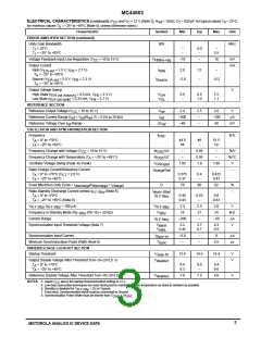
ELECTRICAL CHARACTERISTICS (V
CC
and V = 12 V, [Note 3], R = 10 kΩ, C = 820 pF, for typical values T = 25°C,
for min/max values T = –25° to +85°C [Note 4], unless otherwise noted.)
C
ref
T
A
A
Characteristic
OUTPUT SECTION
Symbol
Min
Typ
Max
Unit
Output Voltage (Note 5)
V
Low State (I
Low State (I
= 100 mA)
= 500 mA)
V
OL
–
–
1.0
1.4
1.2
2.0
Sink
Sink
High State (I
High State (I
= 200 mA)
= 500 mA)
V
OH
–
–
1.5
2.0
2.0
2.7
Source
Source
Output Voltage During Initialization Phase
V
OL
V
V
CC
V
CC
V
CC
= 0 to 1.0 V, I
= 1.0 to 5.0 V, I
= 5.0 to 13 V, I
= 10 µA
–
–
–
–
0.1
0.1
1.0
1.0
1.0
Sink
= 100 µA
Sink
Sink
= 1.0 mA
Output Voltage Rising Edge Slew–Rate (C = 1.0 nF, T = 25°C)
dVo/dT
dVo/dT
–
–
300
–
–
V/µs
V/µs
L
J
Output Voltage Falling Edge Slew–Rate (C = 1.0 nF, T = 25°C)
–300
L
J
ERROR AMPLIFIER SECTION
Voltage Feedback Input (V
= 2.5 V)
V
2.42
–2.0
65
2.5
–0.6
70
2.58
–
V
E/A out
= 2.5 V)
FB
Input Bias Current (V
I
µA
dB
FB
Open Loop Voltage Gain (V
FB–ib
= 2.0 to 4.0 V)
A
VOL
–
E/A out
NOTES: 3. Adjust V
above the startup threshold before setting to 12 V.
CC
4. Low duty cycle pulse techniques are used during test to maintain junction temperature as close to ambient as possible.
5. V must be greater than 5.0 V.
C
2
MOTOROLA ANALOG IC DEVICE DATA

 ONSEMI [ ONSEMI ]