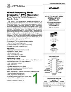
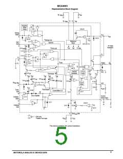
MC44603
ELECTRICAL CHARACTERISTICS (continued) (V
CC
and V = 12 V, [Note 3], R = 10 kΩ, C = 820 pF, for typical values T = 25°C,
C ref T A
for min/max values T = –25° to +85°C [Note 4], unless otherwise noted.)
A
Characteristic
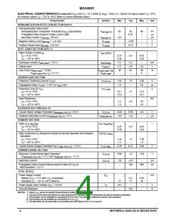
ERROR AMPLIFIER SECTION (continued)
Unity Gain Bandwidth
Symbol
Min
Typ
Max
Unit
BW
MHz
T = 25°C
T = –25° to +85°C
J
–
–
4.0
–
–
5.5
J
Voltage Feedback Input Line Regulation (V
= 10 to 15 V)
V
–10
–
10
mV
mA
CC
FBline–reg
Output Current
Sink (V
T
A
= 1.5 V, V
= 2.7 V)
I
Sink
2.0
12
–
–
E/A out
= –25° to +85°C
FB
Source (V
= 5.0 V, V
= 2.3 V)
I
Source
–2.0
–0.2
E/A out
= –25° to +85°C
FB
T
A
Output Voltage Swing
V
High State (I
Low State (I
= 0.5 mA, V
= 2.3 V)
= 2.7 V)
V
V
OL
5.5
–
6.5
1.0
7.5
1.1
E/A out (source)
= 0.33 mA, V
FB
OH
E/A out (sink)
FB
REFERENCE SECTION
Reference Output Voltage (V
= 10 to 15 V)
V
2.4
–500
–40
2.5
–
2.6
–100
40
V
CC
ref
Reference Current Range (I = V /R , R = 5.0 k to 25 kΩ)
ref ref ref
I
µA
mV
ref
Reference Voltage Over I Range
ref
∆V
–
ref
OSCILLATOR AND SYNCHRONIZATION SECTION
Frequency
f
kHz
OSC
T
T
A
= 0° to +70°C
= –25° to +85°C
44.5
44
48
–
51.5
52
A
Frequency Change with Voltage (V
= 10 to 15 V)
∆f
∆f
/∆V
–
–
0.05
0.05
1.8
–
–
%/V
%/°C
V
CC
OSC
Frequency Change with Temperature (T = –25° to +85°C)
/∆T
OSC
A
Oscillator Voltage Swing (Peak–to–Peak)
V
1.65
1.95
OSC(pp)
Ratio Charge Current/Reference Current
I
/I
–
charge ref
T
T
A
= 0° to +70°C (V
= –25° to +85°C
= 2.0 V)
CT
0.375
0.37
0.4
–
0.425
0.43
A
Fixed Maximum Duty Cycle = I
/(I
R F Stby
+ I
)
D
78
80
82
%
–
discharge discharge charge
Ratio Standby Discharge Current versus I (Note 6)
I
/
disch–Stby
T
T
A
= 0° to +70°C
= –25° to +85°C (Note 8)
I
0.46
0.43
0.53
–
0.6
0.63
A
R F Stby
V
(I
= 100 µA)
V
2.4
18
2.5
21
–
2.6
24
V
kHz
µA
V
R F Stby R F Stby
R F Stby
Frequency in Standby Mode (R
Current Range
(Pin 15) = 25 kΩ)
F
Stby
F Stby
I
–200
–50
R F Stby
Synchronization Input Threshold Voltage (Note 7)
V
V
3.2
0.45
3.7
0.7
4.3
0.9
inthH
inthL
Synchronization Input Current
I
–5.0
–
–
–
0
µA
µs
Sync–in
Minimum Synchronization Pulse Width (Note 8)
UNDERVOLTAGE LOCKOUT SECTION
Startup Threshold
T
Sync
0.5
V
13.6
14.5
15.4
V
V
stup–th
Output Disable Voltage After Threshold Turn–On (UVLO 1)
V
disable1
T
T
A
= 0° to +70°C
= –25° to +85°C
8.6
8.3
9.0
–
9.4
9.6
A
Reference Disable Voltage After Threshold Turn–On (UVLO 2)
V
7.0
7.5
8.0
V
disable2
NOTES: 13. Adjust V
above the startup threshold before setting to 12 V.
CC
14. Low duty cycle pulse techniques are used during test to maintain junction temperature as close to ambient as possible.
16. Standby is disabled for V < 25 mV typical.
R P Stby
17. If not used, Synchronization input must be connected to Ground.
18. Synchronization Pulse Width must be shorter than T
= 1/f .
OSC
OSC
3
MOTOROLA ANALOG IC DEVICE DATA

 ONSEMI [ ONSEMI ]