MC34064, MC33064, NCV33064
MAXIMUM RATINGS
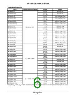
Rating
Symbol
Value
−1.0 to 10
10
Unit
V
Power Input Supply Voltage
Reset Output Voltage
V
in
O
V
V
Reset Output Sink Current (Note 2)
I
Internally
Limited
mA
Sink
Clamp Diode Forward Current, Pin 1 to 2 (Note 2)
I
F
100
mA
Power Dissipation and Thermal Characteristics
P Suffix, Plastic Package
P
625
200
mW
°C/W
D
Maximum Power Dissipation @ T = 25°C
A
R
q
JA
Thermal Resistance, Junction−to−Air
D Suffix, Plastic Package
P
D
625
200
mW
°C/W
Maximum Power Dissipation @ T = 25°C
A
R
q
JA
Thermal Resistance, Junction−to−Air
DM Suffix, Plastic Package
P
D
520
240
mW
°C/W
Maximum Power Dissipation @ T = 25°C
R
A
q
JA
Thermal Resistance, Junction−to−Air
Operating Junction Temperature
T
+150
°C
°C
J
Operating Ambient Temperature
MC34064
T
A
0 to +70
−40 to +85
−40 to +125
MC33064
NCV33064
Storage Temperature Range
T
stg
−65 to +150
°C
Maximum ratings are those values beyond which device damage can occur. Maximum ratings applied to the device are individual stress limit
values (not normal operating conditions) and are not valid simultaneously. If these limits are exceeded, device functional operation is not implied,
damage may occur and reliability may be affected.
1. ESD data available upon request.
ELECTRICAL CHARACTERISTICS (For typical values T = 25°C, for min/max values T is the operating ambient temperature range
A
A
that applies [Notes 3 and 4] unless otherwise noted.)
Characteristics
Symbol
Min
Typ
Max
Unit
COMPARATOR
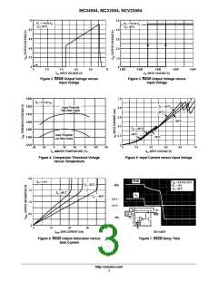
Threshold Voltage
V
High State Output (V Increasing)
Low State Output (V Decreasing)
Hysteresis
V
V
V
4.5
4.5
0.01
4.61
4.59
0.02
4.7
4.7
0.05
in
IH
in
IL
H
RESET OUTPUT
Output Sink Saturation
V
OL
V
(V = 4.0 V, I
= 8.0 mA)
= 2.0 mA)
= 0.1 mA)
−
−
−
0.46
0.15
−
1.0
0.4
0.1
in
Sink
Sink
Sink
(V = 4.0 V, I
in
(V = 1.0 V, I
in
Output Sink Current (V , Reset = 4.0 V)
I
10
−
27
0.02
0.9
60
0.5
1.2
mA
mA
V
in
Sink
Output Off-State Leakage (V , Reset = 5.0 V)
I
OH
in
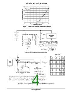
Clamp Diode Forward Voltage, Pin 1 to 2 (I = 10 mA)
V
F
0.6
F
TOTAL DEVICE
Operating Input Voltage Range
V
1.0 to 6.5
−
−
−
V
in
Quiescent Input Current (V = 5.0 V)
I
in
390
500
mA
in
2. Maximum package power dissipation limits must be observed.
3. Low duty cycle pulse techniques are used during test to maintain junction temperature as close to ambient as possible.
4. T
= 0°C for MC34064
−40°C for MC33064
−40°C for NCV33064
T
high
= +70°C for MC34064
+85°C for MC33064
+125°C for NCV33064
low
5. NCV prefix is for automotive and other applications requiring site and change control.
http://onsemi.com
2

 ONSEMI [ ONSEMI ]