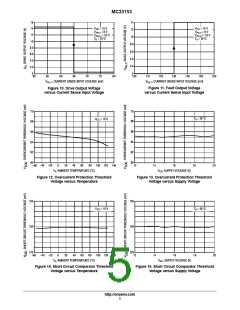
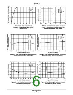
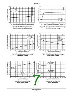
MC33153
APPLICATION INFORMATION
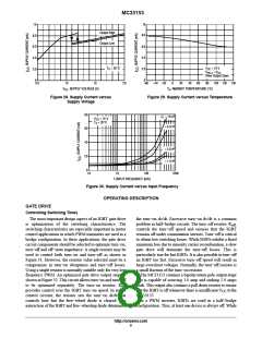
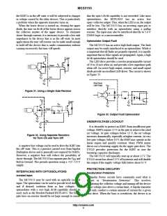
Figure 35 shows a basic IGBT driver application. When
blanking capacitor should be connected from the
driven from an optoisolator, an input pull up resistor is
required. This resistor value should be set to bias the output
transistor at the desired current. A decoupling capacitor
should be placed close to the IC to minimize switching noise.
A bootstrap diode may be used for a floating supply. If the
protection features are not required, then both the Fault
Blanking/Desaturation and Current Sense Inputs should
both be connected to the Kelvin Ground (Pin 2). When used
Desaturation pin to the V pin. If a dual supply is used, the
EE
blanking capacitor should be connected to the Kelvin
Ground. The Current Sense Input should be tied high
because the two comparator outputs are ANDed together.
Although the reverse voltage on collector of the IGBT is
clamped to the emitter by the free−wheeling diode, there is
normally considerable inductance within the package itself.
A small resistor in series with the diode can be used to
protect the IC from reverse voltage transients.
with a single supply, the Kelvin Ground and V pins should
EE
be connected together. Separate gate resistors are
recommended to optimize the turn−on and turn−off drive.
18 V
18 V
6
B+
Bootstrap
8
5
V
Desat/
Blank
7
4
CC
Fault
6
C
Blank
MC33153
V
8
5
CC
Desat/
Blank
Output
7
4
Fault
Output
1
2
Sense
GND
MC33153
Input
V
EE
3
1
2
Sense
GND
Input
V
EE
3
Figure 37. Desaturation Application
Figure 35. Basic Application
When using sense IGBTs or a sense resistor, the sense
voltage is applied to the Current Sense Input. The sense trip
voltages are referenced to the Kelvin Ground pin. The sense
voltage is very small, typically about 65 mV, and sensitive
to noise. Therefore, the sense and ground return conductors
should be routed as a differential pair. An RC filter is useful
in filtering any high frequency noise. A blanking capacitor
15 V
6
V
8
5
CC
Desat/
Blank
is connected from the blanking pin to V . The stray
7
4
EE
Fault
Output
capacitance on the blanking pin provides a very small level
of blanking if left open. The blanking pin should not be
grounded when using current sensing, that would disable the
sense. The blanking pin should never be tied high, that
would short out the clamp transistor.
MC33153
1
2
Sense
GND
Input
V
EE
3
18 V
6
−5.0 V
8
5
V
Desat/
Blank
7
4
CC
Fault
Figure 36. Dual Supply Application
Output
MC33153
When used in a dual supply application as in Figure 36, the
Kelvin Ground should be connected to the emitter of the
IGBT. If the protection features are not used, then both the
Fault Blanking/Desaturation and the Current Sense Inputs
should be connected to Ground. The input optoisolator
1
2
Sense
Input
V
GND
EE
3
should always be referenced to V
.
EE
If desaturation protection is desired, a high voltage diode
is connected to the Fault Blanking/Desaturation pin. The
Figure 38. Sense IGBT Application
http://onsemi.com
11

 ONSEMI [ ONSEMI ]