MC14490
TYPICAL APPLICATIONS
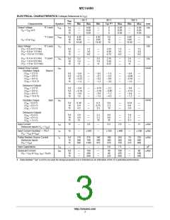
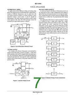
ASYMMETRICAL TIMING
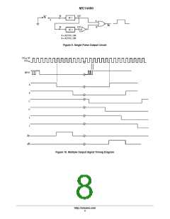
MULTIPLE TIMING SIGNALS
In applications where different leading and trailing edge
delays are required (such as a fast attack/slow release timer.)
Clocks of different frequencies can be gated into the
MC14490 as shown in Figure 6. In order to produce a slow
attack/fast release circuit leads A and B should be
interchanged. The clock out lead can then be used to feed
clock signals to the other MC14490 packages where the
asymmetrical input/output timing is required.
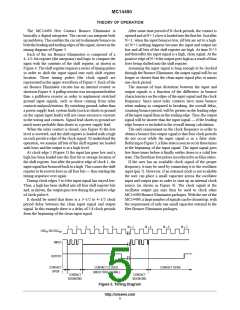
As shown in Figure 8, the Bounce Eliminator circuits can
be connected in series. In this configuration each output is
delayed by four clock periods relative to its respective input.
This configuration may be used to generate multiple timing
signals such as a delay line, for programming other timing
operations.
One application of the above is shown in Figure 9, where
it is required to have a single pulse output for a single
operation (make) of the push button or relay contact. This
only requires the series connection of two Bounce
Eliminator circuits, one inverter, and one NOR gate in order
to generate the signal AB as shown in Figures 9 and 10. The
signal AB is four clock periods in length. If the inverter is
switched to the A output, the pulse AB will be generated
upon release or break of the contact. With the use of a few
additional parts many different pulses and waveshapes may
be generated.
IN
OUT
MC14490
OSC
out
OSC
in
MC14011B
1
15
A
B.E. 1
B.E. 2
B.E. 3
B.E. 4
B.E. 5
B.E. 6
out
A
in
A
B
f
C
EXTERNAL
CLOCK
f
C/N
÷ N
14
2
B
out
B
in
Figure 6. Fast Attack/Slow Release Circuit
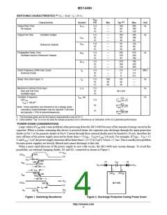
LATCHED OUTPUT
The contents of the Bounce Eliminator can be latched by
using several extra gates as shown in Figure 7. If the latch
lead is high the clock will be stopped when the output goes
low. This will hold the output low even though the input has
returned to the high state. Any time the clock is stopped the
outputs will be representative of the input signal four clock
periods earlier.
3
13
4
C
out
C
in
12
D
out
D
in
5
11
6
E
out
E
in
IN
OUT
10
F
out
F
in
MC14490
OSC
in
OSC
out
MC14011B
7
9
CLOCK
OSC
CLOCK
OSC
out
in
LATCH = 1
UNLATCH = 0
Figure 8. Multiple Timing Circuit Connections
Figure 7. Latched Output Circuit
http://onsemi.com
7

 ONSEMI [ ONSEMI ]