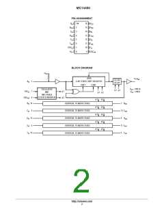
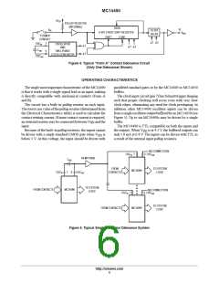
MC14490
+V
DD
PULLUP RESISTOR
(INTERNAL)
DATA
A
15
in
1/2 BIT
DELAY
1
4–BIT STATIC SHIFT REGISTER
A
out
“FORM A”
CONTACT
SHIFT
LOAD
φ1 φ2
7
OSC
OSCILLATOR
AND
TWO–PHASE
CLOCK GENERATOR
in
φ1
φ2
φ1 φ2
C
ext
9
OSC
out
Figure 4. Typical “Form A” Contact Debounce Circuit
(Only One Debouncer Shown)
OPERATING CHARACTERISTICS
The single most important characteristic of the MC14490
is that it works with a single signal lead as an input, making
it directly compatible with mechanical contacts (Form A
and B).
The circuit has a built–in pullup resistor on each input.
The worst case value of the pullup resistor (determined from
the Electrical Characteristics table) is used to calculate the
contact wetting current. If more contact current is required,
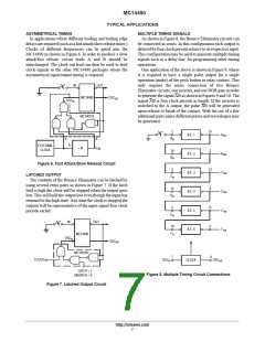
paralleled standard gates or by the MC14049 or MC14050
buffers.
The clock input circuit (pin 7) has Schmitt trigger shaping
such that proper clocking will occur even with very slow
clock edges, eliminating any need for clock preshaping. In
addition, other MC14490 oscillator inputs can be driven
from a single oscillator output buffered by an MC14050 (see
Figure 5). Up to six MC14490s may be driven by a single
buffer.
an external resistor may be connected between V and the
DD
input.
The MC14490 is TTL compatible on both the inputs and
Because of the built–in pullup resistors, the inputs cannot
the outputs. When V is at 4.5 V, the buffered outputs can
DD
be driven with a single standard CMOS gate when V is
below 5 V. At this voltage, the input should be driven with
sink 1.6 mA at 0.4 V. The inputs can be driven with TTL as
a result of the internal input pullup resistors.
DD
NO CONNECTION
OSC
7
9 OSC
in
out
1/6 MC14050
C
ext
FROM
CONTACTS
TO SYSTEM
LOGIC
MC14490
OSC
7
9
OSC
out
in
TO SYSTEM
LOGIC
FROM CONTACTS
MC14490
NO CONNECTION
9 OSC
OSC
7
in
out
TO SYSTEM
LOGIC
FROM CONTACTS
MC14490
Figure 5. Typical Single Oscillator Debounce System
http://onsemi.com
6

 ONSEMI [ ONSEMI ]