MC14490
SWITCHING CHARACTERISTICS (5.) (C = 50 pF, T = 25 C)
L
A
V
Vdc
DD
(6.)
Characteristic
Symbol
Min
Typ
Max
Unit
Output Rise Time
All Outputs
t
5.0
10
15
—
—
—
180
90
65
360
180
130
ns
TLH
Output Fall Time
Oscillator Output
ns
ns
5.0
10
15
—
—
—
100
50
40
200
100
80
t
t
THL
5.0
10
15
—
—
—
60
30
20
120
60
40
THL
Debounce Outputs
Propagation Delay Time
t
5.0
10
15
—
—
—
285
120
95
570
240
190
PHL
PLH
Oscillator Input to Debounce Outputs
t
5.0
10
15
—
—
—
370
160
120
740
320
240
Clock Frequency (50% Duly Cycle)
(External Clock)
f
5.0
10
15
—
—
—
2.8
6
9
1.4
3.0
4.5
MHz
ns
cl
Setup Time (See Figure 1)
t
su
5.0
10
15
100
80
60
50
40
30
—
—
—
Maximum External Clock Input
Rise and Fall Time
t , t
r
5.0
10
15
ns
f
No Limit
Oscillator Input
Oscillator Frequency
f
, typ
Hz
osc
1.5
OSC
5.0
10
15
out
C
(in F)
ext
4.5
(in F)
C
≥ 100 pF*
ext
C
C
Note: These equations are intended to be a design guide.
ext
Laboratory experimentation may be required. Formulas
are typically ± 15% of actual frequencies.
6.5
(in F)
ext
5. The formulas given are for the typical characteristics only at 25 C.
6. Data labelled “Typ” is not to be used for design purposes but is intended as an indication of the IC’s potential performance.
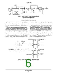
*POWER–DOWN CONSIDERATIONS
Large values of C may cause problems when powering down the MC14490 because of the amount of energy stored in the
ext
capacitor. When a system containing this device is powered down, the capacitor may discharge through the input protection
diodes at Pin 7 or the parasitic diodes at Pin 9. Current through these internal diodes must be limited to 10 mA, therefore the
turn–off time of the power supply must not be faster than t = (V – V
)
SS
C
/(10 mA). For example, If V – V = 15
ext DD SS
DD
VandC =1µF, thepowersupplymustturnoffnofasterthant=(15V) (1µF)/10mA=1.5ms. Thisisusuallynotaproblem
ext
because power supplies are heavily filtered and cannot discharge at this rate.
When a more rapid decrease of the power supply to zero volts occurs, the MC14490 may sustain damage. To avoid this
possibility, use external clamping diodes, D1 and D2, connected as shown in Figure 2.
V
DD
50%
OSC
in
0 V
t
PLH
90%
10%
D1
C
ext
D2
50%
A
out
V
DD
V
DD
t
r
t
7
9
PHL
OSC
90%
10%
OSC
out
in
50%
A
out
t
f
V
DD
OSC
MC14490
in
50%
0 V
t
su
V
0 V
A
in
DD
50%
Figure 1. Switching Waveforms
Figure 2. Discharge Protection During Power Down
http://onsemi.com
4

 ONSEMI [ ONSEMI ]