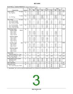
MC14490
THEORY OF OPERATION
The MC14490 Hex Contact Bounce Eliminator is
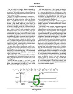
After some time period of N clock periods, the contact is
openedand at N+1 a low is loaded into the first bit. Just after
N+1, when the input bounces low, all bits are set to a high.
At N+2 nothing happens because the input and output are
low and all bits of the shift register are high. At time N+3
and thereafter the input signal is a high, clean signal. At the
positive edge of N+6 the output goes high as a result of four
lows being shifted into the shift register.
Assuming the input signal is long enough to be clocked
through the Bounce Eliminator, the output signal will be no
longer or shorter than the clean input signal plus or minus
one clock period.
The amount of time distortion between the input and
output signals is a function of the difference in bounce
characteristics on the edges of the input signal and the clock
frequency. Since most relay contacts have more bounce
when making as compared to breaking, the overall delay,
counting bounce period, will be greater on the leading edge
of the input signal than on the trailing edge. Thus, the output
signal will be shorter than the input signal — if the leading
edge bounce is included in the overall timing calculation.
The only requirement on the clock frequency in order to
obtain a bounce free output signal is that four clock periods
do not occur while the input signal is in a false state.
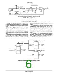
ReferringtoFigure3, afalsestateisseentooccurthreetimes
at the beginning of the input signal. The input signal goes
low three times before it finally settles down to a valid low
state. The first three low pulses are referred to as false states.
If the user has an available clock signal of the proper
frequency, it may be used by connecting it to the oscillator
input (pin 7). However, if an external clock is not available
the user can place a small capacitor across the oscillator
input and output pins in order to start up an internal clock
source (as shown in Figure 4). The clock signal at the
oscillator output pin may then be used to clock other
MC14490 Bounce Eliminator packages. With the use of the
MC14490, a large number of signals can be cleaned up, with
the requirement of only one small capacitor external to the
Hex Bounce Eliminator packages.
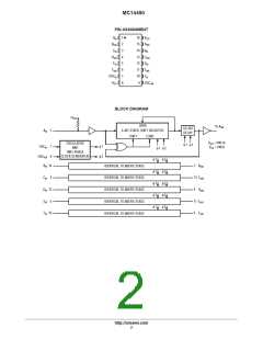
basically a digital integrator. The circuit can integrate both
up and down. This enables the circuit to eliminate bounce on
boththeleadingandtrailingedgesofthesignal, showninthe
timing diagram of Figure 3.
Each of the six Bounce Eliminators is composed of a
4–1/2–bit register (the integrator) and logic to compare the
input with the contents of the shift register, as shown in
Figure 4. The shift register requires a series of timing pulses
in order to shift the input signal into each shift register
location. These timing pulses (the clock signal) are
represented in the upper waveform of Figure 3. Each of the
six Bounce Eliminator circuits has an internal resistor as
shown in Figure 4. A pullup resistor was incorporated rather
than a pulldown resistor in order to implement switched
ground input signals, such as those coming from relay
contacts and push buttons. By switching ground, rather than
a power supply lead, system faults (such as shorts to ground
on the signal input leads) will not cause excessive currents
in the wiring and contacts. Signal lead shorts to ground are
much more probable than shorts to a power supply lead.
When the relay contact is closed, (see Figure 4) the low
level is inverted, and the shift register is loaded with a high
on each positive edge of the clock signal. To understand the
operation, we assume all bits of the shift register are loaded
with lows and the output is at a high level.
At clock edge 1 (Figure 3) the input has gone low and a
high has been loaded into the first bit or storage location of
the shift register. Just after the positive edge of clock 1, the
input signal has bounced back to a high. This causes the shift
register to be reset to lows in all four bits — thus starting the
timing sequence over again.
During clock edges 3 to 6 the input signal has stayed low.
Thus, a high has been shifted into all four shift register bits
and, as shown, the output goes low during the positive edge
of clock pulse 6.
It should be noted that there is a 3–1/2 to 4–1/2 clock
period delay between the clean input signal and output
signal. In this example there is a delay of 3.8 clock periods
from the beginning of the clean input signal.
1
2
3
4
5
6
N + 1
N + 3
N + 5
N + 7
OSC OR OSC
in
out
INPUT
OUTPUT
CONTACT
OPEN
CONTACT CLOSED
CONTACT OPEN
(VALID TRUE SIGNAL)
CONTACT
BOUNCING
CONTACT
BOUNCING
Figure 3. Timing Diagram
http://onsemi.com
5

 ONSEMI [ ONSEMI ]