MC10H109
V
V
B
B
B
B
B
B
B
1
2
3
4
5
6
7
8
16
15
14
13
12
11
10
9
CC1
CC2
out
out
in
4
5
A
out
out
3
2
A
6
7
A
in
in
in
in
9
A
in
10
11
12
13
14
15
A
A
in
in
V
V
V
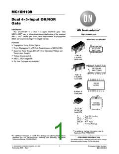
= Pin 1
= Pin 16
= Pin 8
V
CC1
CC2
EE
in
EE
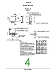
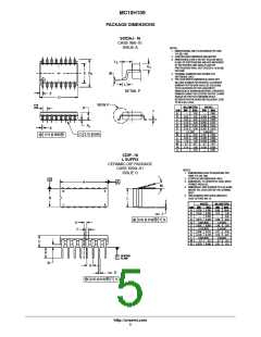
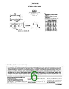
Pin assignment is for Dual−in−Line Package.
Figure 1. Logic Diagram
Figure 2. Pin Assignment
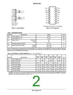
Table 1. MAXIMUM RATINGS
Symbol
Characteristic
Power Supply (V = 0)
Rating
Unit
Vdc
Vdc
mA
V
V
−8.0 to 0
EE
I
CC
Input Voltage (V = 0)
0 to V
CC
EE
I
Output Current
Continuous
50
out
Surge
100
T
Operating Temperature Range
Storage Temperature Range
0 to +75
°C
A
T
stg
Plastic
Ceramic
−55 to +150
−55 to +165
°C
°C
Maximum ratings are those values beyond which device damage can occur. Maximum ratings applied to the device are individual stress limit
values (not normal operating conditions) and are not valid simultaneously. If these limits are exceeded, device functional operation is not implied,
damage may occur and reliability may be affected.
Table 2. ELECTRICAL CHARACTERISTICS (V = −5.2 V 5%) (Note 1)
EE
0°
25°
75°
Symbol
Characteristic
Power Supply Current
Min
−
Max
15
Min
−
Max
14
Min
−
Max
15
Unit
mA
mA
I
I
I
E
Input Current High
Input Current Low
High Output Voltage
Low Output Voltage
High Input Voltage
Low Input Voltage
−
425
−
265
−
265
inH
inL
0.5
−
0.5
−
0.3
−
mA
V
V
V
V
−1.02
−1.95
−1.17
−1.95
−0.84
−1.63
−0.84
−1.48
−0.98
−1.95
−1.13
−1.95
−0.81
−1.63
−0.81
−1.48
−0.92
−1.95
−1.07
−1.95
−0.735
−1.60
−0.735
−1.45
Vdc
Vdc
Vdc
Vdc
OH
OL
IH
IL
1. Each MECL 10H series circuit has been designed to meet the dc specifications shown in the test table, after thermal equilibrium has been
established. The circuit is in a test socket or mounted on a printed circuit board and transverse air flow greater than 500 Ifpm is maintained.
Outputs are terminated through a 50 W resistor to −2.0 V.
http://onsemi.com
2

 ONSEMI [ ONSEMI ]