MC10E122, MC100E122
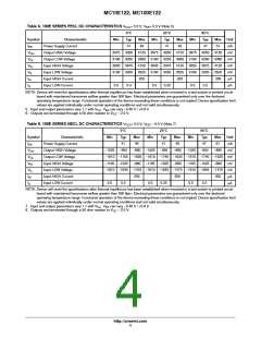
Table 7. AC CHARACTERISTICS V = 5.0 V; V = 0.0 V or V
= 0.0 V; V = −5.0 V (Note 7)
CCx EE
CCx
EE
0°C
25°C
Typ
800
85°C
Typ
800
Symbol
Characteristic
Maximum Toggle Frequency
Propagation Delay to Output
Min
Typ
Max
Min
Max
Min
Max
Unit
MHz
ps
f
t
t
t
800
MAX
PLH
D to Q
150
350
500
150
350
500
150
350
500
PHL
Within-Device Skew
ps
SKEW
D to Q (Note 10)
Random Clock Jitter (RMS)
75
75
75
t
t
t
< 1
< 1
< 1
ps
ps
JITTER
Rise/Fall Times
(20 - 80%)
r
f
300
425
800
300
425
800
300
425
800
NOTE: Device will meet the specifications after thermal equilibrium has been established when mounted in a test socket or printed circuit
board with maintained transverse airflow greater than 500 lfpm. Electrical parameters are guaranteed only over the declared
operating temperature range. Functional operation of the device exceeding these conditions is not implied. Device specification limit
values are applied individually under normal operating conditions and not valid simultaneously.
9. 10 Series: V can vary −0.46 V / +0.06 V.
EE
100 Series: V can vary −0.46 V / +0.8 V.
EE
10.Within-device skew is defined as identical transitions on similar paths through a device.
11. Devices are designed to meet the AC specifications shown in the above table, after thermal equilibrium has been established. The circuit
is in a test socket or mounted on a printed circuit board and transverse air flow greater than 500 lfpm is maintained.
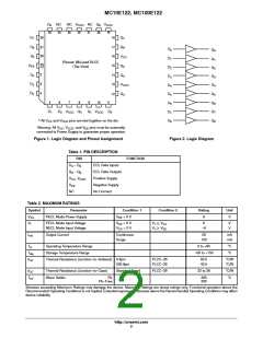
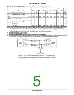
Z = 50 W
Q
Q
D
D
o
Receiver
Device
Driver
Device
Z = 50 W
o
50 W
50 W
V
TT
V
= V − 2.0 V
TT
CC
Figure 3. Typical Termination for Output Driver and Device Evaluation
(See Application Note AND8020/D − Termination of ECL Logic Devices.)
http://onsemi.com
5

 ONSEMI [ ONSEMI ]