MC10E122, MC100E122
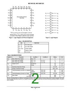
D
8
NC
NC
V
NC
Q
V
CCO
CCO
8
25
24
23
22
21
20
19
D
Q
Q
V
26
18
7
7
6
D
27
28
1
17
16
15
14
13
6
D
0
D
1
D
2
D
3
D
4
D
5
D
6
D
7
D
8
Q
Q
Q
Q
Q
Q
Q
Q
Q
0
1
2
3
4
5
6
7
8
D
5
CC
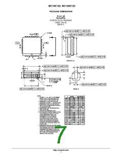
Pinout: 28-Lead PLCC
V
Q
EE
(Top View)
5
4
2
3
4
D
Q
V
4
D
3
CCO
D
2
Q
12
3
5
6
7
8
9
10
11
D
1
D
V
Q
Q
V
Q
0
CCO
0
1
CCO
2
* All V and V
pins are tied together on the die.
CC
CCO
Warning: All V , V
, and V pins must be externally
CCO EE
CC
connected to Power Supply to guarantee proper operation.
Figure 1. Logic Diagram and Pinout Assignment
Figure 2. Logic Diagram
Table 1. PIN DESCRIPTION
PIN
FUNCTION
D
− D
ECL Data Inputs
ECL Data Outputs
Positive Supply
Negative Supply
No Connect
0
8
Q
− Q
0
8
V
V
, V
CCO
CC
EE
NC
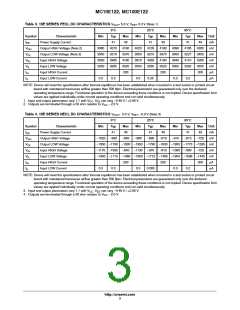
Table 2. MAXIMUM RATINGS
Symbol
Parameter
Condition 1
Condition 2
Rating
Unit
V
V
PECL Mode Power Supply
V
= 0 V
8
V
CC
I
EE
PECL Mode Input Voltage
NECL Mode Input Voltage
V
V
= 0 V
= 0 V
V ꢀ V
6
−6
V
V
EE
CC
I
CC
V ꢁ V
I
EE
I
Output Current
Continuous
Surge
50
100
mA
mA
out
T
Operating Temperature Range
Storage Temperature Range
0 to +85
°C
°C
A
T
−65 to +150
stg
JA
q
Thermal Resistance (Junction−to−Ambient) 0 lfpm
500 lfpm
PLCC−28
PLCC−28
63.5
43.5
°C/W
°C/W
q
Thermal Resistance (Junction−to−Case)
Standard Board
PLCC−28
22 to 26
°C/W
°C
JC
T
sol
Wave Solder
Pb
Pb−Free
265
265
Stresses exceeding Maximum Ratings may damage the device. Maximum Ratings are stress ratings only. Functional operation above the
Recommended Operating Conditions is not implied. Extended exposure to stresses above the Recommended Operating Conditions may affect
device reliability.
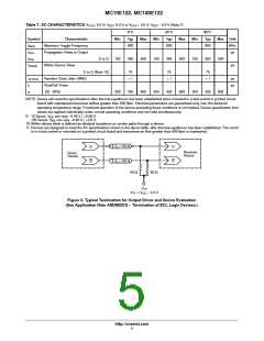
http://onsemi.com
2

 ONSEMI [ ONSEMI ]