MBRS2H100T3G, MBRA2H100T3G
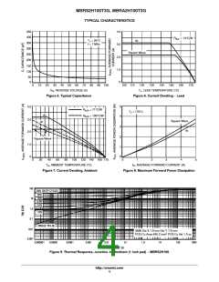
TYPICAL CHARACTERISTICS
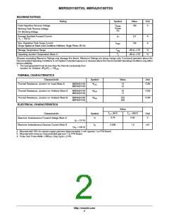
450
400
4.0
R
= 14°C/W
q
JL
T = 25°C
J
dc
350
300
250
200
150
100
f = 1 MHz
3.0
Square Wave
2.0
1.0
0
50
0
0
10 20
30 40 50 60 70 80 90 100
100 110
120
130
140
150
160
170
V , REVERSE VOLTAGE (V)
R
T , LEAD TEMPERATURE (°C)
L
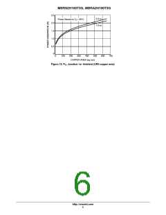
Figure 5. Typical Capacitance
Figure 6. Current Derating − Lead
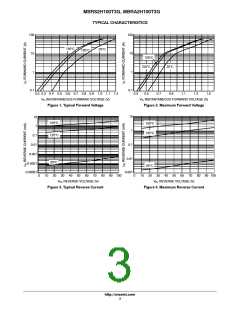
5
4.0
R
R
= 71°C/W
q
q
JA
JA
T = 175°C
J
dc
= 100°C/W
4
3
2
3.0
2.0
Square Wave
dc
dc
Square Wave
1.0
0
1
0
0
1
2
3
4
5
0
20
40
60
80
100 120 140 160 175
I , AVERAGE FORWARD CURRENT (A)
O
T , AMBIENT TEMPERATURE (°C)
A
Figure 8. Maximum Forward Power Dissipation
Figure 7. Current Derating, Ambient
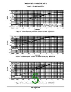
100
50% (DUTY CYCLE)
20%
10%
5.0%
2.0%
10
1.0
0.1
1.0%
SINGLE PULSE
0.01
SMB Die X 1.8 mm Die Y 1.8 mm
PCB Cu Area 645.2 mm PCB Cu thk 1.0 oz
2
0.001
0.000001
0.00001
0.0001
0.001
0.01
PULSE TIME (s)
0.1
1.0
10
100
1000
Figure 9. Thermal Response, Junction−to−Ambient (1 inch pad) − MBRS2H100
http://onsemi.com
4

 ONSEMI [ ONSEMI ]