MBRS2H100T3G, MBRA2H100T3G
MAXIMUM RATINGS
Rating
Symbol
Value
Unit
Peak Repetitive Reverse Voltage
Working Peak Reverse Voltage
DC Blocking Voltage
V
100
V
RRM
RWM
R
V
V
Average Rectified Forward Current
L
I
2.0
A
A
O
(T = 150°C)
Non−Repetitive Peak Surge Current
(Surge Applied at Rated Load Conditions Halfwave, Single Phase, 60 Hz)
I
130
FSM
Storage Temperature Range
T
−65 to +175
−65 to +175
°C
°C
stg
Operating Junction Temperature (Note 1)
T
J
Stresses exceeding Maximum Ratings may damage the device. Maximum Ratings are stress ratings only. Functional operation above the
Recommended Operating Conditions is not implied. Extended exposure to stresses above the Recommended Operating Conditions may affect
device reliability.
1. The heat generated must be less than the thermal conductivity from
Junction−to−Ambient: dP /dT < 1/R .
q
JA
D
J
THERMAL CHARACTERISTICS
Characteristic
Symbol
Value
Unit
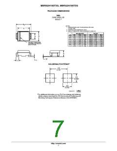
Thermal Resistance, Junction−to−Lead (Note 2)
MBRA2H100
MBRS2H100
Y
R
R
14
12
°C/W
JCL
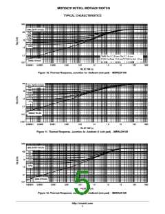
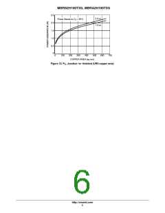
Thermal Resistance, Junction−to−Ambient (Note 2)
Thermal Resistance, Junction−to−Ambient (Note 3)
ELECTRICAL CHARACTERISTICS
MBRA2H100
MBRS2H100
75
71
°C/W
°C/W
q
JA
MBRA2H100
MBRS2H100
275
230
q
JA
Value
T = 25°C
J
T = 125°C
J
Characteristic
Symbol
Unit
v
0.79
0.65
V
Maximum Instantaneous Forward Voltage (Note 4)
F
(i = 2.0 A)
F
Maximum Instantaneous Reverse Current (Note 4)
I
R
0.008
1.5
mA
(V = 100 V)
R
2. Mounted with 700 mm square copper pad size (Approximately 1 inch square) 1 oz FR4 Board.
3. Mounted with minimum recommended pad size 1 oz FR4 Board.
4. Pulse Test: Pulse Width ≤ 380 ms, Duty Cycle ≤ 2.0%.
http://onsemi.com
2

 ONSEMI [ ONSEMI ]