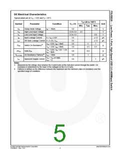
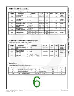
DC Electrical Characteristics
Typical values are at VCC = 3.0V and TA = 25°C.
TA=-40 to +85°C
Symbol
Parameter
Condition
VCC (V)
Unit
Min.
Typ.
Max.
VIK
VIH
VIL
IIN
Clamp Diode Voltage
IIN = -18mA
3.0
3.0 to 3.6
3.0 to 3.6
3.6
-1.2
V
V
High-Level Input Voltage
Low-Level Input Voltage
Input Leakage Current
Off-State Leakage Current
2.0
0.8
±1.0
±1.0
7
V
µA
µA
0 ≤ VIN ≤ 3.6V
0 ≤ A, B ≤ VCC
IOFF
3.6
VIN = 0.8V, ION = 8mA
3.0
5
RON
Switch On Resistance(3)
Ω
VIN = 3.0V, ION = 8mA
3.0
4.5
6.5
VIN = 0.8V, VIN = 0V - 1.5V,
Delta RON
3.0
3.0
3.6
0.3
1
ΔRON
Ω
Ω
I
ON = 8mA
RFLAT(ON) On Resistance Flatness(4) IOUT = 8mA
VIN = VCC or GND,
OUT = 0
ICC
Quiescent Supply Current
1
µA
I
Notes:
3. Measured by the voltage drop between the A and B pins at the indicated current through the switch. On
resistance is determined by the lower of the voltages on the A or B pins.
4. Flatness is defines as the difference between the maximum and the minimum value on resistance over the
specified range of conditions.
© 2005 Fairchild Semiconductor Corporation
FSUSB20 • Rev. 1.0.3
www.fairchildsemi.com
4

 ONSEMI [ ONSEMI ]