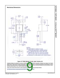
Package Marking and Ordering Information
Device Marking
FQP19N20C
Device
Package
TO-220
Reel Size
Tube
Tape Width
N/A
Quantity
50 units
50 units
FQP19N20C
FQPF19N20C
FQPF19N20C
TO-220F
Tube
N/A
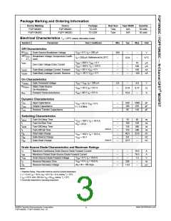
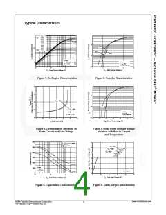
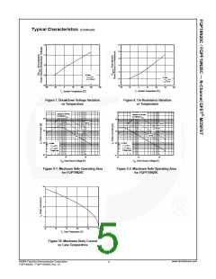
Electrical Characteristics TC = 25oC unless otherwise noted.
Symbol
Parameter
Test Conditions
Min
Typ
Max
Unit
Off Characteristics
BVDSS
VGS = 0 V, ID = 250 μA
Drain-Source Breakdown Voltage
200
--
--
--
--
V
ΔBVDSS
Breakdown Voltage Temperature Coeffi-
I
D = 250 μA, Referenced to 25°C
0.24
V/°C
/
ΔTJ cient
IDSS
V
V
DS = 200 V, VGS = 0 V
DS = 160 V, TC = 125°C
--
--
--
--
--
--
--
--
10
μA
μA
nA
nA
Zero Gate Voltage Drain Current
100
100
-100
IGSSF
IGSSR
VGS = 30 V, VDS = 0 V
VGS = -30 V, VDS = 0 V
Gate-Body Leakage Current, Forward
Gate-Body Leakage Current, Reverse
On Characteristics
VGS(th)
VDS = VGS, ID = 250 μA
Gate Threshold Voltage
2.0
--
--
4.0
0.17
--
V
Ω
S
RDS(on)
Static Drain-Source
On-Resistance
V
GS = 10 V, ID = 9.5 A
0.14
10.8
gFS
VDS = 40 V, ID = 9.5 A
Forward Transconductance
--
Dynamic Characteristics
Ciss
Coss
Crss
Input Capacitance
--
--
--
830
195
85
1080
255
110
pF
pF
pF
VDS = 25 V, VGS = 0 V,
f = 1.0 MHz
Output Capacitance
Reverse Transfer Capacitance
Switching Characteristics
td(on)
tr
td(off)
tf
Turn-On Delay Time
Turn-On Rise Time
Turn-Off Delay Time
Turn-Off Fall Time
Total Gate Charge
Gate-Source Charge
Gate-Drain Charge
--
--
--
--
--
--
--
15
150
135
115
40.5
6.0
40
310
280
240
53.0
--
ns
ns
VDD = 100 V, ID = 19.0 A,
RG = 25 Ω
ns
(Note 4)
(Note 4)
ns
Qg
nC
nC
nC
V
DS = 160 V, ID = 19.0 A,
Qgs
Qgd
VGS = 10 V
22.5
--
Drain-Source Diode Characteristics and Maximum Ratings
IS
Maximum Continuous Drain-Source Diode Forward Current
--
--
--
--
--
--
--
19.0
76.0
1.5
--
A
A
ISM
VSD
trr
Maximum Pulsed Drain-Source Diode Forward Current
VGS = 0 V, IS = 19.0 A
GS = 0 V, IS = 19.0 A,
Drain-Source Diode Forward Voltage
Reverse Recovery Time
--
V
V
208
1.63
ns
μC
dIF / dt = 100 A/μs
Qrr
Reverse Recovery Charge
--
Notes:
1. Repetitive Rating : Pulse width limited by maximum junction temperature.
2. L = 1.8 mH, I = 19.0 A, V = 50 V, R = 25 Ω, starting T = 25°C.
AS
DD
G
J
3. I ≤ 19.0 A, di/dt ≤ 300 A/μs, V ≤ BV
starting T = 25°C.
J
SD
DD
DSS,
4. Essentially independent of operating temperature.
www.fairchildsemi.com
©2004 Fairchild Semiconductor Corporation
FQP19N20C / FQPF19N20C Rev. C1
2

 ONSEMI [ ONSEMI ]