November 2013
FQP19N20C / FQPF19N20C
®
N-Channel QFET MOSFET
200 V, 19 A, 170 mΩ
Features
Description
•
19 A, 200 V, RDS(on) = 170 mΩ (Max.) @ VGS = 10 V,
D = 9.5 A
This N-Channel enhancement mode power MOSFET is
produced using Fairchild Semiconductor’s proprietary
planar stripe and DMOS technology. This advanced
MOSFET technology has been especially tailored to reduce
on-state resistance, and to provide superior switching
performance and high avalanche energy strength. These
devices are suitable for switched mode power supplies,
active power factor correction (PFC), and electronic lamp
ballasts.
I
•
•
•
Low Gate Charge (Typ. 40.5 nC)
Low Crss (Typ. 85 pF)
100% Avalanche Tested
D
G
G
D
S
G
D
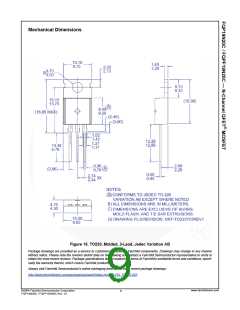
TO-220F
TO-220
S
S
MOSFET Maximum Ratings TC = 25oC unless otherwise noted.
Symbol
VDSS
Parameter
FQP19N20C
FQPF19N20C
Unit
V
Drain to Source Voltage
Drain Current
200
-Continuous (TC = 25oC)
-Continuous (TC = 100oC)
- Pulsed
19.0
12.1
76.0
19.0 *
12.1 *
76.0 *
A
ID
A
IDM
Drain Current
(Note 1)
A
VGSS
EAS
IAR
Gate to Source Voltage
30
433
19.0
13.9
5.5
V
Single Pulsed Avalanche Energy
Avalanche Current
(Note 2)
(Note 1)
(Note 1)
(Note 3)
mJ
A
EAR
dv/dt
Repetitive Avalanche Energy
Peak Diode Recovery dv/dt
mJ
V/ns
W
(TC = 25oC)
- Derate above 25oC
139
43
PD
Power Dissipation
1.11
0.34
W/°C
°C
TJ, TSTG
TL
Operating and Storage Temperature Range
-55 to +150
300
Maximum Lead Temperature for Soldering Purpose,
1/8” from Case for 5 Seconds
°C
*Drain current limited by maximum junction temperature
Thermal Characteristics
Symbol
RθJC
RθJA
Parameter
Unit
°C/W
°C/W
FQP19N20C
FQPF19N20C
2.89
Thermal Resistance, Junction to Case, Max
Thermal Resistance, Junction to Ambient, Max
0.9
62.5
62.5
www.fairchildsemi.com
©2004 Fairchild Semiconductor Corporation
FQP19N20C / FQPF19N20C Rev. C1
1

 ONSEMI [ ONSEMI ]