November 2013
FQP85N06
®
N-Channel QFET MOSFET
60 V, 85 A, 10 mΩ
Description
Features
•
85 A, 60 V, RDS(on) = 10 mΩ (Max.) @ VGS = 10 V,
ID = 42.5 A
This N-Channel enhancement mode power MOSFET is
produced using Fairchild Semiconductor’s proprietary
planar stripe and DMOS technology. This advanced
MOSFET technology has been especially tailored to reduce
on-state resistance, and to provide superior switching
performance and high avalanche energy strength. These
devices are suitable for switched mode power supplies,
audio amplifier, DC motor control, and variable switching
power applications.
•
•
•
•
Low Gate Charge (Typ. 86 nC)
Low Crss (Typ. 165 pF)
100% Avalanche Tested
175°C Maximum Junction Temperature Rating
D
G
G
D
S
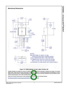
TO-220
S
Absolute Maximum Ratings
T = 25°C unless otherwise noted.
C
Symbol
VDSS
Parameter
FQP85N06
Unit
V
Drain-Source Voltage
60
85
ID
- Continuous (TC = 25°C)
- Continuous (TC = 100°C)
- Pulsed
(Note 5)
(Note 1)
Drain Current
A
60
A
IDM
Drain Current
300
A
VGSS
EAS
IAR
Gate-Source Voltage
25
V
(Note 2)
(Note 1)
(Note 1)
(Note 3)
Single Pulsed Avalanche Energy
Avalanche Current
810
mJ
A
85
EAR
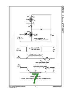
Repetitive Avalanche Energy
Peak Diode Recovery dv/dt
Power Dissipation (TC = 25°C)
16.0
7.0
mJ
V/ns
W
dv/dt
PD
160
- Derate above 25°C
1.07
-55 to +175
W/°C
°C
TJ, TSTG
TL
Operating and Storage Temperature Range
Maximum Lead Temperature for Soldering,
1/8" from Case for 5 seconds
300
°C
Thermal Characteristics
Symbol
Parameter
FQP85N06
0.94
Unit
°C/W
°C/W
RθJC
RθJA
Thermal Resistance, Junction-to-Case, Max.
Thermal Resistance, Junction-to-Ambient, Max.
62.5
www.fairchildsemi.com
©2001 Fairchild Semiconductor Corporation
FQP85N06 Rev. C1
1

 ONSEMI [ ONSEMI ]