FQB10N50CF
®
®
N-Channel QFET FRFET MOSFET
500 V, 10 A, 610 m
Features
Description
•
•
•
•
•
10 A, 500 V, RDS(on) = 610 mΩ (Max.) @ VGS = 10 V, ID = 5 A
Low gate charge ( Typ. 45 nC)
Low Crss ( Typ. 17.5 pF)
This N-Channel enhancement mode power MOSFET is pro-
duced using ON Semiconductor’s proprietary planar stripe and
DMOS technology. This advanced MOSFET technology has
been especially tailored to reduce on-state resistance, and to
provide superior switching performance and high avalanche
energy strength. These devices are suitable for switched mode
power supplies, active power factor correction (PFC), and elec-
tronic lamp ballasts.
100% avalanche tested
Fast recovery body diode
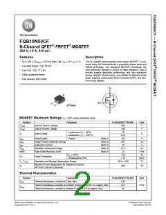
D
D
G
G
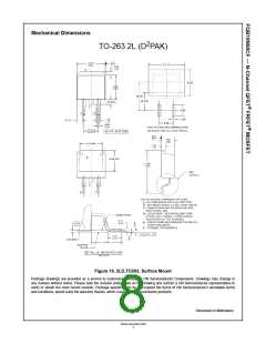
D2-PAK
S
S
MOSFET Maximum Ratings TC = 25oC unless otherwise noted
Symbol
VDSS
VGSS
Parameter
FQB10N50CFTM-WS
Unit
V
Drain to Source Voltage
Gate to Source Voltage
500
±30
V
- Continuous (TC = 25oC)
- Continuous (TC = 100oC)
10
ID
D r a in C u r r e n t
A
6.35
40
IDM
Dr ain Curr ent
- Pu ls ed
(Note 1)
(Note 2)
(Note 1)
(Note 1)
(Note 3)
A
mJ
A
EAS
IAR
Single Pulsed Avalanche Energy
Avalanche Current
825
10
EAR
dv/dt
Repetitive Avalanche Energy
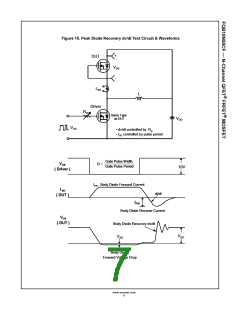
Peak Diode Recovery dv/dt
14.3
2.0
mJ
V/ns
W
W/oC
oC
(TC = 25oC)
- Derate above 25oC
143
PD
Power Dissipation
1.14
-55 to +150
TJ, TSTG
TL
Operating and Storage Temperature Range
Maximum Lead Temperature for Soldering Purpose,
1/8” from Case for 5 Seconds
300
oC
Thermal Characteristics
Symbol
Parameter
Thermal Resistance, Junction to Case, Max
FQB10N50CFTM-WS
Unit
RJC
0.87
62.5
40
Thermal Resistance, Junction to Ambient (minimum pad of 2 oz copper), Max.
Thermal Resistance, Junction to Ambient (1 in2 pad of 2 oz copper), Max.
oC/W
RJA
©2010 Semiconductor Components Industries, LLC
September-2017, Rev. 3
Publication Order Number:
FQB10N50CFTM-WS

 ONSEMI [ ONSEMI ]