February 2009
FDS8842NZ
N-Channel PowerTrench® MOSFET
40 V, 14.9 A, 7.0 mΩ
Features
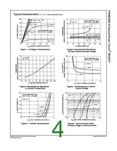
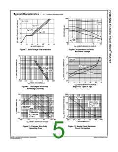
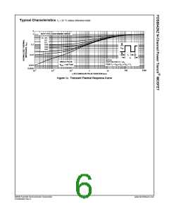
General Description
Max rDS(on) = 7.0 mΩ at VGS = 10 V, ID = 14.9 A
Max rDS(on) = 11.6 mΩ at VGS = 4.5 V, ID = 11.6 A
HBM ESD protection level of 4.4 kV typical(note 3)
The FDS8842NZ has been designed to minimize losses in
power conversion application. Advancements in both silicon and
package technologies have been combined to offer the lowest
rDS(on) while maintaining excellent switching performance.
High performance trench technology for extremely low rDS(on)
and fast switching
Applications
Synchronous Buck for Notebook Vcore and Server
Notebook Battery
High power and current handling capability
Termination is Lead-free and RoHS Compliant
Load Switch
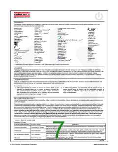
D
D
D
G
D
D
D
D
S
S
G
SO-8
S
S
D
S
Pin 1
S
MOSFET Maximum Ratings TA = 25 °C unless otherwise noted
Symbol
VDS
VGS
Parameter
Ratings
40
Units
Drain to Source Voltage
Gate to Source Voltage
Drain Current -Continuous
-Pulsed
V
V
±20
14.9
ID
A
93
EAS
PD
Single Pulse Avalanche Energy
Power Dissipation
(Note 4)
(Note 1a)
(Note 1b)
253
mJ
W
TA = 25 °C
TA = 25 °C
2.5
Power Dissipation
1.0
TJ, TSTG
Operating and Storage Junction Temperature Range
-55 to +150
°C
Thermal Characteristics
RθJC
RθJA
Thermal Resistance, Junction to Case
Thermal Resistance, Junction to Ambient
(Note 1)
25
50
°C/W
(Note 1a)
Package Marking and Ordering Information
Device Marking
Device
Package
Reel Size
Tape Width
12 mm
Quantity
FDS8842NZ
FDS8842NZ
SO8
13 ’’
2500 units
1
©2009 Fairchild Semiconductor Corporation
FDS8842NZ Rev.C
www.fairchildsemi.com

 ONSEMI [ ONSEMI ]