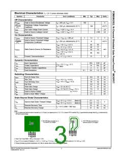
Electrical Characteristics TJ = 25 °C unless otherwise noted
Symbol
Parameter
Test Conditions
Min
Typ
Max
Units
Off Characteristics
BVDSS
Drain to Source Breakdown Voltage
ID = 250 μA, VGS = 0 V
150
V
ΔBVDSS
ΔTJ
Breakdown Voltage Temperature
Coefficient
ID = 250 μA, referenced to 25 °C
104
mV/°C
IDSS
IGSS
Zero Gate Voltage Drain Current
Gate to Source Leakage Current
VDS = 120 V, VGS = 0 V
VGS = ±20 V, VDS = 0 V
1
μA
±100
nA
On Characteristics
VGS(th)
Gate to Source Threshold Voltage
VGS = VDS, ID = 250 μA
1
1.5
-6
3
V
ΔVGS(th)
ΔTJ
Gate to Source Threshold Voltage
Temperature Coefficient
I
D = 250 μA, referenced to 25 °C
mV/°C
V
GS = 10 V, ID = 4.4 A
46
48
52
56
71
75
VGS = 6 V, ID = 3.8 A
VGS = 4.5 V, ID = 3.7 A
rDS(on)
Static Drain to Source On Resistance
Forward Transconductance
mΩ
VGS = 10 V, ID = 4.4 A,
TJ = 125 °C
90
21
110
gFS
VDS = 5 V, ID = 4.4 A
S
Dynamic Characteristics
Ciss
Coss
Crss
Rg
Input Capacitance
952
74
3
1335
105
5
pF
pF
pF
Ω
VDS = 75 V, VGS = 0 V,
f = 1 MHz
Output Capacitance
Reverse Transfer Capacitance
Gate Resistance
0.1
0.6
1.8
Switching Characteristics
td(on)
tr
td(off)
tf
Turn-On Delay Time
Rise Time
6.8
1.4
19
14
10
34
10
21
11
ns
ns
VDD = 75 V, ID = 4.4 A,
V
GS = 10 V, RGEN = 6 Ω
Turn-Off Delay Time
Fall Time
ns
2.9
15
ns
Qg
Total Gate Charge
Total Gate Charge
Gate to Source Charge
Gate to Drain “Miller” Charge
VGS = 0 V to 10 V
VGS = 0 V to 4.5 V
nC
nC
nC
nC
Qg
7.6
2.1
2.3
VDD = 75 V,
D = 4.4 A
I
Qgs
Qgd
Drain-Source Diode Characteristics
V
GS = 0 V, IS = 1.9 A
(Note 2)
(Note 2)
0.7
0.8
53
1.2
1.3
85
VSD
Source-Drain Diode Forward Voltage
V
VGS = 0 V, IS = 4.4 A
trr
Reverse Recovery Time
ns
IF = 4.4 A, di/dt = 100 A/μs
Qrr
Reverse Recovery Charge
51
82
nC
Notes:
2
1. R
is determined with the device mounted on a 1 in pad 2 oz copper pad on a 1.5 x 1.5 in. board of FR-4 material. R
is guaranteed by design while R is determined by
θCA
θJA
θJC
the user's board design.
a.
50 °C/W when mounted on a
1 in pad of 2 oz copper
125 °C/W when mounted on a
minimum pad of 2 oz copper.
b.
2
2. Pulse Test: Pulse Width < 300 μs, Duty cycle < 2.0%.
3. E of 73 mJ is based on Starting T = 25 °C, L = 3 mH, I = 7 A, V = 150 V, V = 10 V. 100% tested at L =0.1 mH, I = 24 A.
AS
J
AS
DD
GS
AS
4. Pulsed Id limited by junction temperature, td<=100 μS, please refer to SOA curve for more details.
©2013 Fairchild Semiconductor Corporation
FDMS86252L Rev.C2
www.fairchildsemi.com
2

 ONSEMI [ ONSEMI ]