October 2014
FDMS86252L
N-Channel Shielded Gate PowerTrench® MOSFET
150 V, 12 A, 56 mΩ
Features
General Description
This N-Channel MOSFET is produced using Fairchild
Semiconductor’s
Shielded Gate MOSFET Technology
advanced PowerTrench® process that
Max rDS(on) = 56 mΩ at VGS = 10 V, ID = 4.4 A
Max rDS(on) = 71 mΩ at VGS = 6 V, ID = 3.8 A
Max rDS(on) = 75 mΩ at VGS = 4.5 V, ID = 3.7 A
incorporates Shielded Gate technology. This process has been
optimized for the on-state resistance and yet maintain superior
switching performance.
Applications
Advanced package and silicon combination for low rDS(on) and
high efficiency
OringFET / Load Switching
Synchronous Rectification
DC-DC Conversion
Next generation enhanced body diode technol-
ogy, engineered for soft recovery
MSL1 robust package design
100% UIL tested
RoHS Compliant
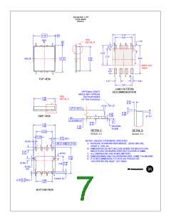
Bottom
Top
Pin 1
S
S
D
D
D
D
Pin 1
S
S
G
S
S
G
D
D
D
D
Power 56
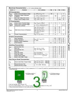
MOSFET Maximum Ratings TA = 25 °C unless otherwise noted
Symbol
VDS
VGS
Parameter
Ratings
Units
Drain to Source Voltage
Gate to Source Voltage
Drain Current -Continuous
-Continuous
150
V
V
±20
TC = 25 °C
TA = 25 °C
12
ID
(Note 1a)
(Note 4)
(Note 3)
4.4
A
-Pulsed
30
EAS
Single Pulse Avalanche Energy
Power Dissipation
73
50
mJ
W
TC = 25 °C
TA = 25 °C
PD
Power Dissipation
(Note 1a)
2.5
TJ, TSTG
Operating and Storage Junction Temperature Range
-55 to +150
°C
Thermal Characteristics
RθJC
RθJA
Thermal Resistance, Junction to Case
Thermal Resistance, Junction to Ambient
2.5
50
°C/W
(Note 1a)
Package Marking and Ordering Information
Device Marking
Device
Package
Reel Size
13 ’’
Tape Width
12 mm
Quantity
FDMS86252L
FDMS86252L
Power 56
3000 units
©2013 Fairchild Semiconductor Corporation
FDMS86252L Rev.C2
www.fairchildsemi.com
1

 ONSEMI [ ONSEMI ]