FCPF190N65FL1−F154
ELECTRICAL CHARACTERISTICS (T = 25°C unless otherwise noted)
C
Symbol
Parameter
Test Conditions
Min.
Typ.
Max.
Unit
OFF CHARACTERISTICS
BV
Drain to Source Breakdown Voltage
650
700
−
−
−
−
−
−
V
V
V
V
I
= 0 V, I = 10 mA, T = 25_C
DSS
GS
D
J
= 0 V, I = 10 mA, T = 150_C
GS
D
J
ꢃ
B
V
/
ꢃ
T
Breakdown Voltage Temperature
Coefficient
= 10 mA, Referenced to 25_C
0.72
V/_C
DSS
J
D
I
Zero Gate Voltage Drain Current
V
V
V
= 650 V, V = 0 V
−
−
−
−
60
−
10
−
ꢁ A
ꢁ A
V
DSS
DS
DS
GS
GS
= 520 V, V = 0 V, T = 125_C
GS
C
I
Gate to Body Leakage Current
=
20 V, V = 0 V
100
GSS
DS
ON CHARACTERISTICS
V
Gate Threshold Voltage
V
GS
V
GS
V
DS
= V , I = 2 mA
3
−
−
−
5
190
−
GS(th)
DS(on)
DS
D
R
Static Drain to Source On Resistance
Forward Transconductance
= 10 V, I = 10 A
168
18
mꢀ
D
g
= 20 V, I = 10 A
S
FS
D
DYNAMIC CHARACTERISTICS
C
Input Capacitance
V
= 100 V, V = 0 V, f = 1 MHz
−
−
−
−
−
−
−
−
−
2350
77
3055
100
−
pF
pF
pF
pF
pF
nC
nC
nC
ꢀ
iss
DS
GS
C
Output Capacitance
oss
C
Reverse Transfer Capacitance
Output Capacitance
0.68
44
rss
C
V
DS
V
DS
V
DS
= 380 V, V = 0 V, f = 1 MHz
−
oss
GS
C
Effective Output Capacitance
Total Gate Charge at 10 V
Gate to Source Gate Charge
Gate to Drain “Miller” Charge
Equivalent Series Resistance
= 0 V to 400 V, V = 0 V
304
60
−
oss(eff.)
GS
Q
= 380 V, I = 10 A, V = 10 V
78
−
g(tot)
D
GS
(Note 4)
Q
12
gs
gd
Q
25
−
ESR
f = 1 MHz
0.6
−
SWITCHING CHARACTERISTICS
t
Turn-On Delay Time
Turn-On Rise Time
Turn-Off Delay Time
Turn-Off Fall Time
V
= 380 V, I = 10 A, V = 10 V,
−
−
−
−
25
11
60
32
ns
ns
ns
ns
d(on)
DD
g
D
GS
R = 4.7
ꢀ
t
r
(Note 4)
t
62
4.2
134
18
d(off)
t
f
SOURCE−DRAIN DIODE CHARACTERISTICS
I
Maximum Continuous Source to Drain Diode Forward Current
Maximum Pulsed Source to Drain Diode Forward Current
−
−
−
−
−
−
−
20.6
61.8
1.2
−
A
A
S
I
SM
V
SD
Source to Drain Diode Forward Voltage
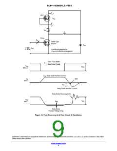
Reverse Recovery Time
V
V
= 0 V, I = 10 A
−
V
GS
SD
t
rr
= 400 V, I = 10 A,
105
515
ns
nC
DD
SD
dI /dt = 100 A/ꢁ s
F
Q
Reverse Recovery Charge
−
rr
Product parametric performance is indicated in the Electrical Characteristics for the listed test conditions, unless otherwise noted. Product
performance may not be indicated by the Electrical Characteristics if operated under different conditions.
4. Essentially independent of operating temperature.
www.onsemi.com
3

 ONSEMI [ ONSEMI ]