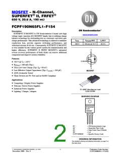
FCPF190N65FL1−F154
ABSOLUTE MAXIMUM RATINGS (T = 25°C, Unless otherwise noted)
C
Symbol
Parameter
Value
650
Unit
V
V
DSS
V
GSS
Drain to Source Voltage
Gate to Source Voltage
− DC
20
V
− AC (f > 1 Hz)
30
I
Drain Current
− Continuous (T = 25°C)
20.6
13.1
61.8
400
A
D
C
− Continuous (T = 100°C)
C
I
Drain Current
− Pulsed (Note 1)
A
mJ
A
DM
E
Single Pulsed Avalanche Energy (Note 2)
Avalanche Current (Note 2)
Repetitive Avalanche Energy (Note 1)
MOSFET dv/dt
AS
AS
I
4
E
AR
0.39
100
mJ
V/ns
dv/dt
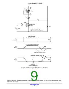
Peak Diode Recovery dv/dt (Note 3)
Power Dissipation
50
P
(T = 25°C)
39
W
W/°C
°C
D
C
− Derate Above 25°C
0.31
−55 to +150
300
T , T
Operating and Storage Temperature Range
J
STG
T
Maximum Lead Temperature for Soldering, 1/8″ from Case for 5 Seconds
°C
L
Stresses exceeding those listed in the Maximum Ratings table may damage the device. If any of these limits are exceeded, device functionality
should not be assumed, damage may occur and reliability may be affected.
1. Repetitive rating: pulse width limited by maximum junction temperature.
2. I = 4A, R = 25 ꢀ, starting T = 25°C.
AS
G
J
3. I ≤ 10 A, di/dt ≤ 200 A/ꢁ s, V ≤ 380 V, starting T = 25°C.
SD
DD
J
THERMAL CHARACTERISTICS
Symbol
Parameter
Value
3.2
Unit
R
Thermal Resistance, Junction to Case, Max.
Thermal Resistance, Junction to Ambient, Max.
_C/W
_C/W
ꢂ
JC
JA
R
62.5
ꢂ
PACKAGE MARKING AND ORDERING INFORMATION
Part Number
Top Marking
Package
Shipping
50 Units / Tube
FCPF190N65FL1−F154
FCPF190N65F
TO−220F
(Pb−Free)
www.onsemi.com
2

 ONSEMI [ ONSEMI ]