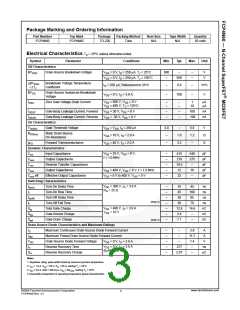
Typical Performance Characteristics
Figure 1. On-Region Characteristics
Figure 2. Transfer Characteristics
VGS
101
10
Top :
15.0 V
10.0 V
8.0V
7.5 V
7.0 V
6.5 V
6.0 V
150oC
Bottom : 5.5 V
1
100
25oC
-55oC
* Notes :
1. 250µs Pulse Test
* Note
1. VDS = 40V
o
2. TC = 25 C
0.1
2. 250µs Pulse Test
10-1
0.1
1
10
2
4
6
8
10
VDS, Drain-Source Voltage [V]
VGS , Gate-Source Voltage [V]
Figure 3. On-Resistance Variation vs.
Drain Current and Gate Voltage
Figure 4. Body Diode Forward Voltage
Variation vs. Source Current
and Temperatue
4
3
101
VGS = 10V
2
100
150oC
VGS = 20V
25oC
1
* Notes :
1. VGS = 0V
* Note : TJ = 25oC
10.0
2. 250µs Pulse Test
10-1
0.2
0
0.0
2.5
5.0
7.5
12.5
0.4
0.6
0.8
1.0
1.2
ID, Drain Current [A]
VSD , Source-Drain Voltage [V]
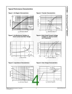
Figure 5. Capacitance Characteristics
Figure 6. Gate Charge Characteristics
1200
12
Ciss = Cgs + Cgd (Cds = shorted)
VDS = 120V
Coss = Cds + Cgd
Crss = Cgd
VDS = 300V
VDS = 480V
1000
800
600
400
200
0
10
8
* Notes :
1. VGS = 0 V
6
4
2
Coss
Ciss
2. f = 1 MHz
* Note : ID = 3.9A
Crss
0
100
101
0
5
10
15
VDS, Drain-Source Voltage [V]
QG, Total Gate Charge [nC]
www.fairchildsemi.com
©2008 Fairchild Semiconductor Corporation
FCP4N60 Rev. C1
3

 ONSEMI [ ONSEMI ]