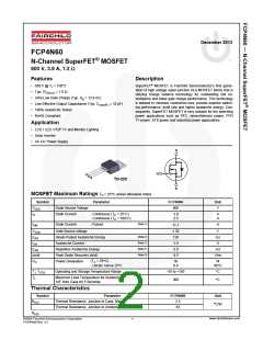
Package Marking and Ordering Information
Part Number
Top Mark
Package
Packing Method
Reel Size
Tape Width
Quantity
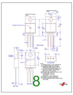
FCP4N60
FCP4N60
TO-220
Tube
N/A
N/A
50 units
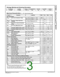
Electrical Characteristics TC = 25oC unless otherwise noted.
Symbol
Parameter
Conditions
Min.
Typ.
Max.
Unit
Off Characteristics
BVDSS
Drain-Source Breakdown Voltage
VGS = 0 V, ID = 250 µA, TJ = 25°C
VGS = 0 V, ID = 250 µA, TJ = 150°C
600
--
--
--
--
V
V
650
∆BVDSS
/ ∆TJ
Breakdown Voltage Temperature
Coefficient
ID = 250 µA, Referenced to 25°C
--
--
0.6
--
--
V/°C
BVDS
Drain-Source Avalanche Breakdown
Voltage
VGS = 0 V, ID = 3.9 A
700
V
VDS = 600 V, VGS = 0 V
VDS = 480 V, TC = 125°C
IDSS
Zero Gate Voltage Drain Current
--
--
--
--
1
10
µA
µA
IGSSF
IGSSR
Gate-Body Leakage Current, Forward
Gate-Body Leakage Current, Reverse
VGS = 30 V, VDS = 0 V
VGS = -30 V, VDS = 0 V
--
--
--
--
100
nA
nA
-100
On Characteristics
VGS(th) Gate Threshold Voltage
RDS(on)
VDS = VGS, ID = 250 µA
VGS = 10 V, ID = 2.0 A
VDS = 40 V, ID = 2.0 A
3.0
--
--
5.0
1.2
--
V
Ω
S
Static Drain-Source
On-Resistance
1.0
3.2
gFS
Forward Transconductance
--
Dynamic Characteristics
VDS = 25 V, VGS = 0 V,
f = 1.0 MHz
Ciss
Input Capacitance
--
--
--
--
--
415
210
19.5
12
540
275
--
pF
pF
pF
pF
pF
Coss
Output Capacitance
Crss
Reverse Transfer Capacitance
Output Capacitance
Coss
VDS = 480 V, VGS = 0 V, f = 1.0 MHz
VDS = 0 V to 400 V, VGS = 0 V
16
--
Coss eff.
Effective Output Capacitance
32
Switching Characteristics
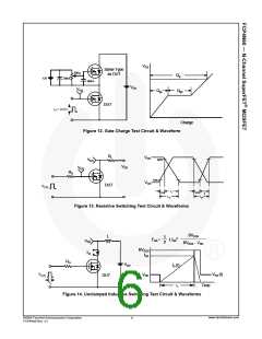
td(on) Turn-On Delay Time
tr
td(off)
tf
VDD = 300 V, ID = 3.9 A
RG = 25 Ω
--
--
--
--
--
--
--
16
45
45
100
85
ns
ns
Turn-On Rise Time
Turn-Off Delay Time
Turn-Off Fall Time
Total Gate Charge
Gate-Source Charge
Gate-Drain Charge
36
ns
(Note 4)
30
70
ns
VDS = 480 V, ID = 3.9 A
VGS = 10 V
Qg
12.8
2.4
7.1
16.6
--
nC
nC
nC
Qgs
Qgd
--
(Note 4)
Drain-Source Diode Characteristics and Maximum Ratings
IS
Maximum Continuous Drain-Source Diode Forward Current
Maximum Pulsed Drain-Source Diode Forward Current
--
--
--
--
--
--
--
3.9
11.7
1.4
--
A
A
ISM
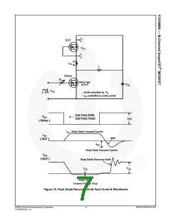
VSD
trr
Drain-Source Diode Forward Voltage
Reverse Recovery Time
VGS = 0 V, IS = 3.9 A
--
V
VGS = 0 V, IS = 3.9 A
277
2.07
ns
µC
dIF/dt =100 A/µs
Qrr
Reverse Recovery Charge
--
Notes:
1. Repetitive rating: pulse-width limited by maximum junction temperature.
2. I = 1.9 A, V = 50 V, R = 25 Ω, starting T = 25°C.
AS
DD
G
J
3. I ≤ 3.9 A, di/dt ≤ 200 A/µs, V ≤ BV
, starting T = 25°C.
SD
DD
DSS
J
4. Essentially independent of operating temperature typical characteristics.
www.fairchildsemi.com
©2008 Fairchild Semiconductor Corporation
FCP4N60 Rev. C1
2

 ONSEMI [ ONSEMI ]