December 2013
FCP4N60
N-Channel SuperFET MOSFET
®
600 V, 3.9 A, 1.2 Ω
Features
Description
•
•
•
•
•
•
650 V @ TJ = 150°C
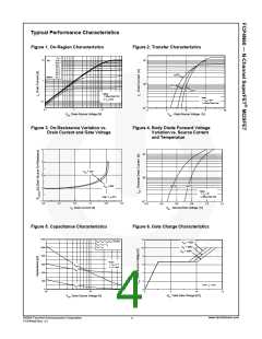
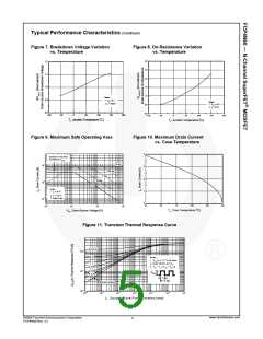
SuperFET® MOSFET is Fairchild Semiconductor’s first gener-
ation of high voltage super-junction (SJ) MOSFET family that is
utilizing charge balance technology for outstanding low on-
resistance and lower gate charge performance. This technology
is tailored to minimize conduction loss, provide superior switch-
ing performance, dv/dt rate and higher avalanche energy. Con-
sequently, SuperFET MOSFET is very suitable for the switching
power applications such as PFC, server/telecom power, FPD
TV power, ATX power and industrial power applications.
Typ. RDS(on) = 1.0 Ω
Ultra Low Gate Charge (Typ. Qg = 12.8 nC)
Low Effective Output Capacitance (Typ. Coss(eff.) = 32 pF)
100% Avalanche Tested
RoHS Compliant
Application
•
•
•
LCD / LED / PDP TV and Monitor Lighting
Solar Inverter
AC-DC Power Supply
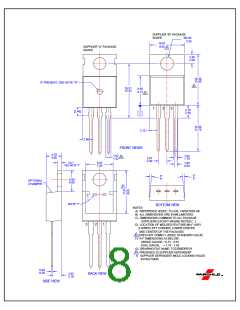
D
G
G
D
S
TO-220
S
MOSFET Maximum Ratings TC = 25oC unless otherwise noted.
Symbol
VDSS
Parameter
FCP4N60
Unit
Drain-Source Voltage
Drain Current
600
V
ID
- Continuous (TC = 25°C)
- Continuous (TC = 100°C)
3.9
2.5
A
A
(Note 1)
IDM
Drain Current
- Pulsed
A
11.7
± 30
128
3.9
VGSS
EAS
IAR
Gate-Source voltage
V
mJ
A
(Note 2)
(Note 1)
(Note 1)
(Note 3)
Single Pulsed Avalanche Energy
Avalanche Current
EAR
dv/dt
PD
Repetitive Avalanche Energy
Peak Diode Recovery dv/dt
5.0
mJ
V/ns
4.5
(TC = 25°C)
Power Dissipation
50
W
- Derate Above 25°C
0.4
W/°C
TJ, TSTG
TL
Operating and Storage Temperature Range
-55 to +150
300
°C
Maximum Lead Temperature for Soldering,
1/8” from Case for 5 Seconds.
°C
Thermal Characteristics
Symbol
Parameter
FCP4N60
2.5
Unit
RθJC
Thermal Resistance, Junction to Case, Max.
Thermal Resistance, Junction to Ambient, Max.
oC/W
83
RθJA
www.fairchildsemi.com
©2008 Fairchild Semiconductor Corporation
FCP4N60 Rev. C1
1

 ONSEMI [ ONSEMI ]