CAT1021, CAT1022, CAT1023
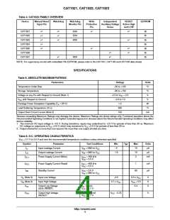
Table 4. CAT102X FAMILY OVERVIEW
Device
Manual Reset
Input Pin
Watchdog
Watchdog
Monitor Pin
Write
Protection
Pin
Independent
Auxiliary Voltage
Sense
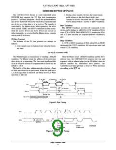
RESET:
Active High
and LOW
EEPROM
CAT1021
CAT1022
CAT1023
CAT1024
CAT1025
CAT1026
CAT1027
n
n
n
n
n
n
n
n
SDA
SDA
WDI
n
n
2k
2k
2k
2k
2k
2k
2k
n
n
n
n
n
n
n
WDI
NOTE: For supervisory circuits with embedded 16k EEPROM, please refer to the CAT1161, CAT1162 and CAT1163 data sheets.
SPECIFICATIONS
Table 5. ABSOLUTE MAXIMUM RATINGS
Parameters
Ratings
Units
°C
°C
V
Temperature Under Bias
Storage Temperature
–55 to +125
–65 to +150
Voltage on any Pin with Respect to Ground (Note 1)
with Respect to Ground
−2.0 to V + 2.0
CC
V
CC
−2.0 to 7.0
1.0
V
Package Power Dissipation Capability (T = 25°C)
W
A
Lead Soldering Temperature (10 s)
Output Short Circuit Current (Note 2)
300
°C
mA
100
Stresses exceeding Maximum Ratings may damage the device. Maximum Ratings are stress ratings only. Functional operation above the
Recommended Operating Conditions is not implied. Extended exposure to stresses above the Recommended Operating Conditions may affect
device reliability.
1. The minimum DC input voltage is –0.5 V. During transitions, inputs may undershoot to –2.0 V for periods of less than 20 ns. Maximum
DC voltage on output pins is V +0.5 V, which may overshoot to V +2.0 V for periods of less than 20 ns.
CC
CC
2. Output shorted for no more than one second. No more than one output shorted at a time.
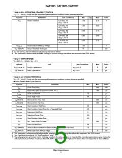
Table 6. D.C. OPERATING CHARACTERISTICS
V
CC
= 2.7 V to 5.5 V and over the recommended temperature conditions unless otherwise specified.
Symbol
Parameter
Input Leakage Current
Test Conditions
Min
−2
Typ
Max
10
10
3
Units
mA
I
LI
V
V
= GND to V
= GND to V
IN
CC
CC
I
LO
Output Leakage Current
−10
mA
IN
I
Power Supply Current (Write)
f
= 400 kHz
= 5.5 V
mA
CC1
SCL
V
CC
I
Power Supply Current (Read)
Standby Current
f
= 400 kHz
= 5.5 V
1
60
mA
CC2
SCL
CC
V
I
V
V
= 5.5 V
= GND to V
mA
SB
CC
IN
CC
V
(Note 3)
(Note 3)
Input Low Voltage
Input High Voltage
−0.5
0.3 x V
V
V
V
IL
CC
V
IH
0.7 x V
V
CC
+ 0.5
CC
V
OL
Output Low Voltage
(SDA, RESET)
I
= 3 mA
CC
0.4
OL
V
= 2.7 V
V
OH
Output High Voltage
(RESET)
I
= −0.4 mA
CC
V − 0.75
CC
V
OH
V
= 2.7 V
http://onsemi.com
4

 ONSEMI [ ONSEMI ]