ADP3212/NCP3218
PIN CONFIGURATION AND FUNCTION DESCRIPTIONS
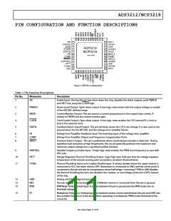
Figure 3. QFN Pin Configuration
Table 3. Pin Function Descriptions
Pin No.
1
Mnemonic
EN
Description
Enable Input. Driving this pin low shuts down the chip, disables the driver outputs, pulls PWRGD
and VRTT low, and pulls high.
CLKEN
2
3
4
5
PWRGD
IMON
Power-Good Output. Open-drain output. A low logic state means that the output voltage is outside
of the VID DAC defined range.
Current Monitor Output. This pin sources a current proportional to the output load current. A
resistor to FBRTN sets the current monitor gain.
Clock Enable Output. Open-drain output. A low logic state enables the CPU internal PLL clock to
lock to the external clock.
Feedback Return Input/Output. This pin remotely senses the CPU core voltage. It is also used as the
ground return for the VID DAC and the voltage error amplifier blocks.
CLKEN
FBRTN
6
7
8
FB
COMP
TRDET
Voltage Error Amplifier Feedback Input. The inverting input of the voltage error amplifier.
Voltage Error Amplifier Output and Frequency Compensation Point.
Transient Detect Output. This pin is pulled low when a load release transient is detected. During
repetitive load transients at high frequencies, this circuit optimally positions the maximum and
minimum output voltage into a specified loadline window.
9
VARFREQ
VRTT
Variable Frequency Enable Input. A high logic state enables the PWM clock frequency to vary with
VID code.
Voltage Regulator Thermal Throttling Output. Logic high state indicates that the voltage regulator
temperature at the remote sensing point exceeded a set alarm threshold level.
Thermal Throttling Sense and Crowbar Disable Input. A resistor divider where the upper resistor is
connected to VCC, the lower resistor (NTC thermistor) is connected to GND, and the center point is
connected to this pin and acts as a temperature sensor half bridge. Connecting TTSNS to GND disables
the thermal throttling function and disables the crowbar, or overvoltage protection (OVP), feature
of the chip.
10
11
TTSNS
12
13
14
GND
IREF
RPM
Analog and Digital Signal Ground.
This pin sets the internal bias currents. A 80kohm resistor is connected from this pin to ground.
RPM Mode Timing Control Input. A resistor between this pin to ground sets the RPM mode turn-on
threshold voltage.
15
RT
Multiphase Frequency Setting Input. An external resistor connected between this pin and GND sets
the oscillator frequency of the device when operating in multiphase PWM mode.threshold of the
converter.
Rev. SpA | Page 11 of 43

 ONSEMI [ ONSEMI ]