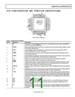
ADP3212/NCP3218
Pin No.
Mnemonic
Description
16
RAMP
PWM Ramp Slope Setting Input. An external resistor from the converter input voltage node to this
pin sets the slope of the internal PWM stabilizing ramp used for phase-current balancing.
17
18
LLINE
Output Load Line Programming Input. The center point of a resistor divider between CSREF and
CSCOMP is connected to this pin to set the load line slope.
Current Sense Reference Input. This pin must be connected to the common point of the output
inductors. The node is shorted to GND through an internal switch when the chip is disabled to
provide soft stop transient control of the converter output voltage.
CSREF
19
20
21
22
CSSUM
CSCOMP
ILIM
Current Sense Summing Input. External resistors from each switch node to this pin sum the
inductor currents to provide total current information.
Current-Sense Compensation Point. A resistor and capacitor from this pin to CSSUM determine the
gain of the current-sense amplifier and the positioning loop response time.
Current-Limit Setpoint. An external resistor from this pin to CSCOMP sets the current-limit threshold of
the converter.
Multiphase Output Disable Logic Output. This pin is actively pulled low when the ADP3212/NCP3218
enters single-phase mode or during shutdown. Connect this pin to the SD inputs of the Phase-3
MOSFET drivers.
OD3
23
24
25
PWM3
SWFB3
BST2
Logic-Level PWM Output for phase 3. Connect to the input of an external MOSFET driver such as the
ADP3611.
Current Balance Input for phase 3. Input for measuring the current level in phase 3. SWFB3 should
be left open for 1 or 2 phase configuration.
High-Side Bootstrap Supply for Phase 2. A capacitor from this pin to SW2 holds the bootstrapped
voltage while the high-side MOSFET is on.
26
27
28
DRVH2
SW2
SWFB2
High-Side Gate Drive Output for Phase 2.
Current Return for High-Side Gate Drive for phase 2.
Current Balance Input for phase 2. Input for measuring the current level in phase 2. SWFB2 should
be left open for 1 phase configuration.
29
30
31
32
33
34
35
36
DRVL2
PGND
DRVL1
PVCC
SWFB1
SW1
Low-Side Gate Drive Output for Phase 2.
Low-Side Driver Power Ground
Low-Side Gate Drive Output for Phase 1..
Power Supply Input/Output of Low-Side Gate Drivers.
Current Balance Input for phase 1. Input for measuring the current level in phase 1.
Current Return For High-Side Gate Drive for phase 1.
High-Side Gate Drive Output for Phase 1.
High-Side Bootstrap Supply for Phase 1. A capacitor from this pin to SW1 holds the bootstrapped
voltage while the high-side MOSFET is on.
DRVH1
BST1
37
38
39
VCC
PH1
PH0
Power Supply Input/Output of the Controller.
Phase Number Configuration Input. Connect to VCC for 3 phase configuration.
Phase Number Configuration Input. Connect to GND for 1 phase configuration. Connect to VCC for
multiphase configuration.
40
41
DPRSLP
PSI
Deeper Sleep Control Input.
Power State Indicator Input. Pulling this pin to GND forces the ADP3212/NCP3218 to operate in
single-phase mode.
42 to 48
VID6 to VID0
Voltage Identification DAC Inputs. When in normal operation mode, the DAC output programs the
FB regulation voltage from 0.3 V to 1.5 V (see Table 6).
Rev. SpA | Page 12 of 43

 ONSEMI [ ONSEMI ]