September 2000
Revised June 2005
74LCXH16244
Low Voltage 16-Bit Buffer/Line Driver with Bushold
General Description
Features
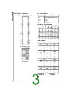
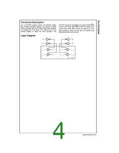
The LCXH16244 contains sixteen non-inverting buffers
with 3-STATE outputs designed to be employed as a mem-
ory and address driver, clock driver, or bus oriented trans-
mitter/receiver. The device is nibble controlled. Each nibble
has separate 3-STATE control inputs which can be shorted
together for full 16-bit operation.
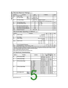
■ 5V tolerant control inputs and outputs
■ 2.3V–3.6V VCC specifications provided
■ 4.5 ns tPD max (VCC 3.0V), 20 A ICC max
■ Bushold on inputs eliminates the need for external
pull-up/pull-down resistors
The LCXH16244 data inputs include active bushold cir-
cuitry, eliminating the need for external pull-up resistors to
hold unused or floating data inputs at a valid logic level.
■ Power down high impedance inputs and outputs
■
24 mA output drive (VCC 3.0V)
■ Implements proprietary noise/EMI reduction circuitry
■ Latch-up performance exceeds 500 mA
■ ESD performance:
The LCXH16244 is designed for low voltage (2.5V or 3.3V)
VCC applications with capability of interfacing to a 5V signal
environment.
Human body model 2000V
The LCXH16244 is fabricated with an advanced CMOS
technology to achieve high speed operation while maintain-
ing CMOS low power dissipation.
Machine model 200V
■ Also packaged in plastic Fine-Pitch Ball Grid Array
(FBGA)
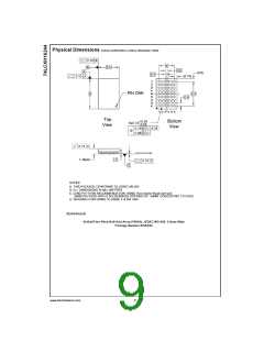
Ordering Code:
Order Number
Package Number
Package Description
74LCXH16244G
(Note 1)(Note 2)
BGA54A
54-Ball Fine-Pitch Ball Grid Array (FBGA), JEDEC MO-205, 5.5mm Wide
74LCXH16244MEA
(Note 2)
MS48A
MTD48
48-Lead Small Shrink Outline Package (SSOP), JEDEC MO-118, 0.300" Wide
48-Lead Thin Shrink Small Outline Package (TSSOP), JEDEC MO-153, 6.1mm Wide
74LCXH16244MTD
(Note 2)
Note 1: Ordering code “G” indicates Trays.
Note 2: Devices also available in Tape and Reel. Specify by appending the suffix letter “X” to the ordering code.
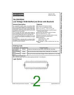
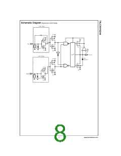
Logic Symbol
© 2005 Fairchild Semiconductor Corporation
DS500248
www.fairchildsemi.com

 ONSEMI [ ONSEMI ]