AMIS-52150 Low-Power Transceiver with Clock and Data Recovery
Data Sheet
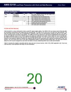
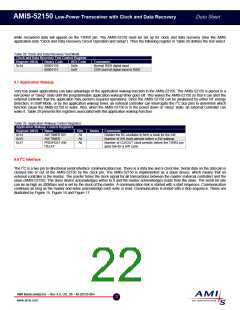
Table 27: Data and Clock Recovery Control Registers
Data and Clock Recovery Associated Registers
Register (HEX)
0x07
0x08
0x09
0x0d
Name
FWORD LSB
FWORD
FWORD MSB
DATA MUX
Bits
All
All
All
6
States
Comments
Sets the initial internal clock frequency for the clock and data
recovery circuits
0
TX/RX normal signals
1
0
1
Recovered data on TX/RX
Normal CLKOUT signals
Recovered CLOCK output on CLKOUT
Filter coefficient gain is 1
Filter coefficient gain is 2
Filter coefficient gain is 4
Filter coefficient gain is 8
Filter coefficient gain is 16
Filter coefficient gain is 32
Filter coefficient gain is 64
Filter coefficient gain is 128
Filter coefficient gain is 1
Filter coefficient gain is 2
Filter coefficient gain is 4
Filter coefficient gain is 8
Filter coefficient gain is 16
Filter coefficient gain is 32
Filter coefficient gain is 64
Filter coefficient gain is 128
Filter coefficient gain is 0.125
Filter coefficient gain is 0.250
Filter coefficient gain is 0.500
Filter coefficient gain is 1.000
Filter coefficient gain is 2
Filter coefficient gain is 4
Filter coefficient gain is 8
Filter coefficient gain is 16
Sample frequency divider is 2
Sample frequency divider is 4
Sample frequency divider is 8
Sample frequency divider is 16
Sample frequency divider is 20
Sample frequency divider is 32
Sample frequency divider is 40
Sample frequency divider is 48
StopCheck bits: disabled
StopCheck bits: 2
CLKMUX
K0
7
0x10
0x11
0x12
0,1,2
000
001
010
011
100
101
110
111
000
001
010
011
100
101
110
111
000
001
010
011
100
101
110
111
000
001
010
011
100
101
110
111
00
K1
4,5,6
0,1,2
4,5,6
K2
FsDIV
STOP CHECK
LOOPCLAMP
0,1
2,3
01
10
StopCheck bits: 4
11
StopCheck bits: 8
00
01
10
11
0
1
0
Loop clamp value is: +-BaudClk/8
Loop clamp value is: +-BaudClk/16
Loop clamp value is: +-BaudClk/32
Loop clamp value is: +-BaudClk/64
Phase alignment enabled
Phase alignment disabled
CDR reset disabled
FREERUN
4
5
6
7
CRD RESET
1
CDR reset enabled
AUTO/MANUAL
RESET
SAMPLE
WINDOW
0
POR reset (auto)
1
00
00
CDR reset enabled (manual)
Sampling starts with bit start edge
Sampling centered around bit center
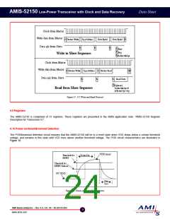
The clock and data recovery function requires that the receiver be able to recover the data from the incoming RF signal. There is a
method to test the clock and data recovery function without having to set the receiver up to receive data. This is a test mode that allows
an input data stream (square wave at 1/2 the data rate) to be input on the RSSI pin and recovered clock will appear on the CLKOUT pin
AMI Semiconductor – Rev 4.0, Oct. 06 – M-20535-004
21
www.amis.com

 ONSEMI [ ONSEMI ]