AMIS-52150 Low-Power Transceiver with Clock and Data Recovery
Data Sheet
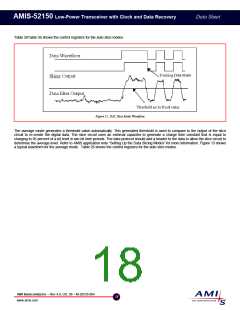
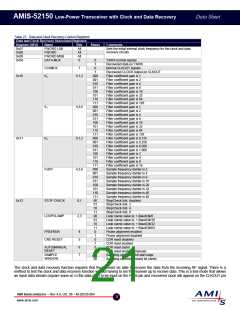
Table 26: Auto Slice Control Registers
Auto Slice Control Registers
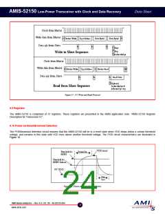
Register (HEX)
Name
Bits
States
Comments
0x0a
DATA SLICE
THRESHOLD
HYSTERESIS
All
Set a fixed reference level for the slice output to be
compared to in the DAC mode
0x0f
0,1
00
01
10
11
00
01
10
11
0mV hysteresis used in the threshold circuit
20mV hysteresis used in the threshold circuit
50mV hysteresis used in the threshold circuit
100mV hysteresis used in the threshold circuit
DAC mode used for data detection (DEFAULT)
Average mode used for data detection
Peak mode used for data detection
AUTOSLICE
2,3
DAC mode used for data detection
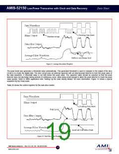
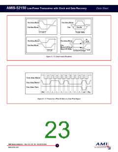
9.6 Data and Clock Recovery
Data recovered in a noisy environment or from a small RF signal usually is jittery. The AMIS-52150 can remove much of that data jitter
by recovering a synchronous clock signal from the incoming data. The AMIS-52150 can be set to do auto slice data detection. The
clock and data recovery circuits can be programmed to generate a data clock for synchronously clocking the data out of the AMIS-
52150, removing much of the jitter in this process. The AMIS-52150 has an internal PLL that must be programmed to the frequency of
the data by setting the values in the FWORD register and setting the coefficients of the filter. If these values are close to the data rate,
the AMIS-52150 will recover the data clock from the incoming detected data. The CDR circuit can also be set or clamped with a
tolerance to the frequency difference between the supposed data rate and the actual data rate to improve the performance of the CDR
function. The CDR circuit can be set to reset after a programmed number of data time periods without data. This stop check function
allows the CDR circuit to reacquire the clock when new data is received, maintaining better clock to data synchronization.
Table 27 presents the registers associated with the data and clock recovery function. Refer to the AMIS application note “Clock and
Data Recovery Circuit Operation and Setup” for more information.
AMI Semiconductor – Rev 4.0, Oct. 06 – M-20535-004
20
www.amis.com

 ONSEMI [ ONSEMI ]