AMIS-52150 Low-Power Transceiver with Clock and Data Recovery
Data Sheet
while recovered data will appear on the TX/RX pin. The AMIS-52150 must be set up for clock and data recovery (See the AMIS
application note “Clock and Data Recovery Circuit Operation and Setup”). Then the following register in Table 28 defines the test select.
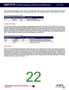
Table 28: Clock and Data Recovery Test Mode
Clock and Data Recovery Test Control Register
Register (HEX)
0x1d
Binary Code
00001110
00001111
HEX Code
0x0e
0x0f
Comments
Normal RSSI digital input
CDR start bit digital input to RSSI
9.7 Application Wakeup
Very low power applications can take advantage of the application wakeup function in the AMIS-52150. The AMIS-52150 is placed in a
low power or “sleep” state until the programmable application wakeup timer goes off. This wakes the AMIS-52150 so that it can alert the
external controller that the application may perform required operations. Since the AMIS-52150 can be awakened by either RF energy
detection, in Sniff Mode, or by the application wakeup timer, an external controller can interrogate the I2C bus pins to determine which
function cause the AMIS-52150 to wake. Also, when the AMIS-52150 is in the power down or “sleep’ state, an external controller can
wake it. Table 29 presents the registers associated with this application wakeup function.
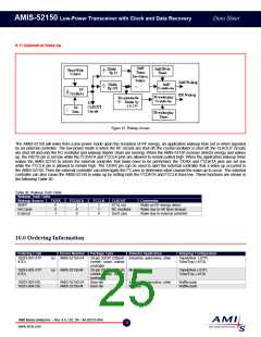
Table 29: Application Wakeup Control Registers
Application Wakeup Control Registers
Register (HEX)
0x14
0x15
Name
Bits
All
All
States
Comments
AW TIMER DIV
AW TIMER
PRE/POST AW
DELAY
Divides the RC oscillator to form a clock for the AW
Number of AW clock periods before a AW wakeup
Number of CLKOUT clock periods before the TX/RX pin
goes low for a AW cycle
0x17
All
9.8 I2C Interface
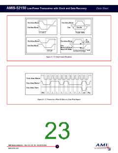
The I2C is a two pin bi-directional serial interface communication bus. There is a data line and a clock line. Serial data on the data pin is
clocked into or out of the AMIS-52150 by the clock pin. The AMIS-52150 is implemented as a slave device, which means that an
external controller is the master. The master forms the clock signal for all transactions between the master (external controller) and the
slave (AMIS-52150). The slave device acknowledges writes to it and the master acknowledges reads from the slave. The serial bit rate
can be as high as 400Kbps and is set by the clock of the master. A communication link is started with a start sequence. Communication
continues as long as the master and slave acknowledge each write or read. Communication is ended with a stop sequence. These are
illustrated by Figure 15, Figure 16 and Figure 17.
AMI Semiconductor – Rev 4.0, Oct. 06 – M-20535-004
22
www.amis.com

 ONSEMI [ ONSEMI ]