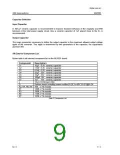
PEDL5501-02
OKI Semiconductor
ML5501
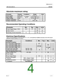
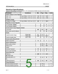
Electrical Specifications
Typicals and limits appearing in normal type apply for TJ = 25°C. Limits appearing in Boldface type apply over the entire junction
temperature range for operation, 0°C to 125°C.
Parameter
Conditions
Min.
Typ.
Max.
Units
Output Voltage of Linear Regulator
Vout = 12 V
0<Iout<300mA, 10.8V<Vin<13.2V
0<Iout<300mA, 10.8V<Vin<13.2V
11.40
16.15
12.0
17.0
12.60
17.85
V
V
Vout = 17V
Feedback Voltage
Feedback Pin Voltage
Regulation of Linear Regulator
Line Regulation (Note2)
Load Regulation (Note1)
0<Iout<300mA, 10.8V<Vin<13.2V
0.95
400
1.0
1.050
V
0.5
1.0
%
%
Current Limit of Linear Regulator (Note4)
Current limit
600
900
50
mA
mA
Short circuit current (Foldback)
Enable
Rising edge
Falling edge
Enss = Gnd
0.7
0.9
0.5
1.1
0.65
1.7
Enable threshold voltage
V
0.35
Current in disable mode
Current Limit of Boost DC-DC
Switch Current limit
Switch ON-Resistance
NMOS switch of Boost
PMOS of LDO
mA
1.3
3
A
300
500
750
mΩ
mΩ
1500
UVLO
Vdd Start Threshold
Vdd Turn off Threshold
Internal Band Gap
Reference
7.5
6
9
8
10.5
10
V
V
0.965
1.0
90
1.035
95
V
%
Max Duty Cycle
Max duty cycle at 17V
Fs
Switching frequency
Thermal Shutdown
Thermal shutdown trip point
Thermal shutdown hysteresis
300
350
400
KHz
150
30
°C
°C
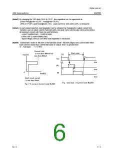
Rev 1.0
5 / 13

 OKI [ OKI ELECTRONIC COMPONETS ]