PEDL5501-02
OKI Semiconductor
ML5501
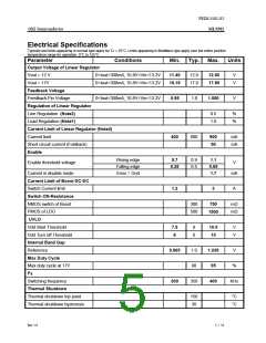
THERMAL INFORMATION
Implementation of integrated circuits in low-profile and fine-pitch surface-mount packages typically
requires special attention to power dissipation. Many system-dependent issues such as thermal
coupling, airflow, added heat sinks and convection surfaces and the presence of other heat-generating
components affect the power-dissipation limits of a given component.
Three basic approaches for enhancing thermal performance are listed below:
• Improving the power dissipation capability of the PCB design
• Improving the thermal coupling of the component to the PCB
• Introducing airflow in the system
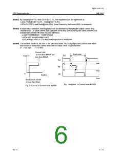
The ML5501 regulator has internal thermal shutdown to protect the device from over-heating. Under all
possible operating conditions, the junction temperature of the ML5501 must be within the range of 0 °C
to 125 °C. For high power applications a heatsink is required since the package alone will not dissipate
enough heat to satisfy this requirement (TJ(max) ≤125°C). This heatsink is the combination of the
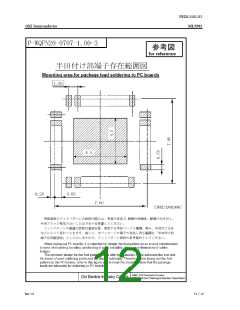
mounting pad directly below the chip and at least one ground plane at the bottom side of PCB. At least
nine vias (12 is preferable) with 0.3-0.33 mm diameter and 1.2 mm pitch must be used for connecting
the mounting pad to bottom plate. Using a 4-layer board according to JESD51-7 is highly recommended
in high power application (Figure 4). By using this structure a θJA of 30 °C/W is achievable.
Figure 4: PCB specifications according to JESD51-7
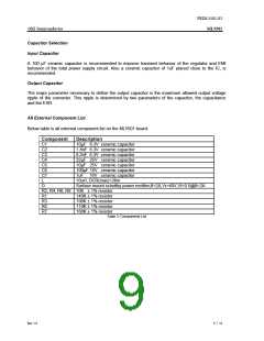
LAYOUT CONSIDERATIONS
High switching frequencies and large peak currents make PC board layout a critical part of design. Poor
design will cause excessive EMI and ground bounce, both of which can cause instability or regulation
errors by corrupting the voltage and current feedback signals.
Power components (such as the inductor, converter IC, filter capacitors, and output diode) should be
placed as close together as possible, and their traces should be kept short, direct, and wide. Connect
the inductor from the battery to the SW pins as close to the IC as possible. Keep the voltage feedback
network very close to the IC, within 0.2in (5mm) of the FB pins. Keep noisy traces, such as those from
the SW pin, away from the voltage feedback networks and guarded from them using grounded copper.
Rev 1.0
10 / 13

 OKI [ OKI ELECTRONIC COMPONETS ]